WaveForms ROM logic
The core of any of the instrumentation Digilent devices (Electronics Explorer, Analog Discovery, Analog Discovery 2, Digital Discovery, etc.) is an FPGA circuit loaded with the associated configuration file. The WaveForms software communicates with the FPGA and provides user interfaces as a workbench of instruments.
The Digital Pattern Generator (Patterns) instrument handles the DIO (Digital Input/Output) pins of the FPGA. It allows defining three types of output I/O objects: Signal, Bus or ROM logic. Multiple objects of same or different types can be built.
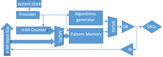
The figure below shows the block diagram associated with a single DIO pin. The Input Buffers (IB) and Output Buffers (OB) are intrinsic to the FPGA IO bank structure. The Pattern Memory is implemented in the FPGA block RAM. All other blocks are implemented in the programmable area of the FPGA.
A DIO line can be set as Output in at most one Pattern Generator object. When a line is used by the Static I/O as an output element (Slider, Button, or Switch), this has priority over the signal configuration in Patterns (not shown in the block diagram).
Signals and Buses generate time sequenced output values: the sampling rate derives from the system clock, and the sample values are either algorithmically generated (clocks, pulses, counters, etc.) or read from a Pattern Memory (custom). In the latter case, a Counter points the current sample in the Pattern Memory.
For the ROM logic, a Boolean function Truth Table is stored in the Pattern Memory. An n-bit input bus (from DIO pins) builds the address for the Pattern Memory. Consequently, it generates the output values as Boolean function of DIO arguments. In the figure below, MUX2 selects Pattern Memory, and MUX1 selects the n-bit input bus.
Since the size of the Pattern Memory is limited to 2n locations, the input buffer IB is only present for the first n DIO pins (0 to n-1). However, any DIO pin can implement a Boolean function of DIO pins 0 to n-1.
For Analog Discovery, Analog Discovery 2 and Electronics Explorer default configurations, n = 10, meaning that only DIO0…DIO9 can be used as inputs in ROM logic blocks. Alternate configurations for these devices extend n = 14. For Digital Discovery, n = 15.
Since the Pattern Memory is implemented in an FPGA Block RAM, the Boolean function is synchronized on the prescaled clock.
Figure 1 DIO pin block diagram.
1. Using ROM logic to implement combinatorial Boolean functions
As long as none of the DIO pins defined as outputs in a ROM logic object is also used as input in the same object, there is no feedback path and the Boolean function is combinatorial. However, the output is synchronized to the prescaled clock.
Figure 2 ROM Logic implementing a set of combinatorial functions.
2. Using ROM logic to implement sequential Boolean functions
A DIO pin used as input (argument) in its own Boolean function closes a feedback loop, and the DIO pin is a state bit. One or more state bits build a state variable in a Finite State Machine (FSM).
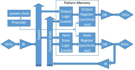
The figure below shows the generic block diagram of a Mealy FSM mapped on a ROM logic object. A Moore FSM does not use the Inputs in Output Logic block.
Notice that the pins used both as inputs and outputs (DIOx) form the State Variable; the pins used as inputs only (DIOy) are FSM inputs and the pins used as outputs only (DIOz) are FSM (synchronized) outputs. The state variable is always available at the FPGA DIOx pins.
The FSM can be implemented in a single or in multiple ROM logic objects. In the latter case, a clean design would use a ROM logic object for the Next State Logic and the State Register, and another one for the Output Logic and the Output Register.
Figure 3 ROM Logic implementing a Mealy State Machine.
3. ROM logic User Interface in WaveForms
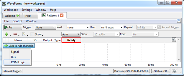
In the Pattern Generator, click the green “plus” sign and select ROM logic, as shown below.
Figure 4 Opening a new ROM logic object.
In the Pop-up window, select the Properties tab. Select or type in the synchronizing frequency. Use the green “plus” signs to add input and output signals in the left and right lists. Use the green arrows to move signals up or down in the lists. The list order will be preserved in the Truth Table tab.
Select the Truth Table tab. Edit or import the truth table. Use the Truth Table rules:
- Change the signal names in the Properties tab, if convenient (optional). Changed names will be used in the Truth Table.
- If a signal is used in both input and output panes, it is a State Variable; the input pane shows its value in the Current State and the output pane indicates its value in the Next State.
- Use 0, 1 or X (don’t care) in the input pane.
- An expanded Truth Table (no X input values) with n input signals has 2n lines. A line including k X values is the collapsed version of 2k lines of the expanded Truth Table.
- Make sure that all possible input cases are covered, i.e. the logical reunion of all input lines is 2n.
- Use 1, 0, “SignalName” or “/SignalName” in the output pane. “SignalName” is the name of one of the signals in the input pane. “/” stands for logical NOT.
- The table lines are “sequential”, i.e. a line can override lines above it in the table. For example, the first line in the table might be used to describe the default output values, while subsequent lines override particular cases.
- The same functional block might be split in multiple ROM logic objects, to optimize the Truth Table(s).
- A yellow background of a cell indicates a syntax error.
The rules and ROM logic GUI operation is demonstrated in the following examples.
4. Example: Three input, synchronous AND gate.
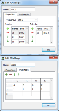
In Figure 5, the ROM logic object is named AND3 (optional). DIO0…DIO2 are selected as inputs, DIO3 as output. The signal names are changed to i0…i2, respectively o3 (optional). The synchronizing frequency is set to 5MHz, meaning the output signal will be synchronized to a 5MHz clock with 0° phase, relative to the moment of running the Pattern Generator; this way, the output signal is synchronized to other signals generated by the Pattern generator.
In the Truth Table tab, the first line describes the default case, with the output signal value of 0. With three X-es in the input pane, this line is equivalent to 23=8 expanded lines. However, the second line overrides one line out of the eight, forcing the output signal to 1 when all inputs are 1. The equivalent VHDL code is:
 -- Line 1 in the truth table
 AND3: process(i2,i1,i0)
 begin
    o3 <= ‘0’;  -- default output is ‘0’
 -- Line 2 in the truth table
    if i2 = ‘1’ and i1 = ‘1’ and i0 = ‘1’ then
       o3 <= ‘1’; -- overrides o3 for a particular case
    end if;
 end process;
Notice that the Truth Table lines are “sequential”, with the same meaning as the lines within a VHDL process: a line can override the effect of previous lines, in both cases.
Figure 5 Synchronous 3 input AND gate ROM logic.
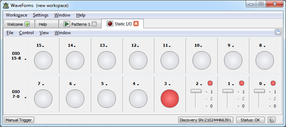
To verify the behavior of the 3 input AND gate, Run the Pattern Generator and the Static IO. Set the DIO2…DIO0 as Switches and keep DIO3 as LED, in the Static IO. Notice that DIO3 is High only when all DIO2, DIO1 and DIO0 are High. Make sure you close the Static IO.
Figure 6. Using Static IO to verify the 3 input synchronized AND gate.
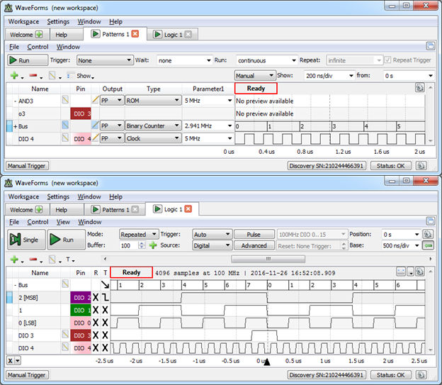
To observe the dynamic behavior of the synchronized 3-input AND gate, define a binary counter on DIO2…DIO0 in the Pattern Generator. Set the clock frequency to 3MHz. (However, the closest frequency WaveForms can generate is 2.941MHz.) This frequency is chosen not to be integer multiple or submultiple of the ROM logic frequency (5MHz). Also define a 5MHz clock on DIO4 (same as for the ROM logic). This clock is not used by the ROM logic, but will serve as reference for observation in the Logic Analyzer.
Open a Logic Analyzer. Add/Bus with DIO2…DIO0, and Add/Signals DIO3 and DIO4. Set the trigger on the falling edge of DIO2. Set convenient time base and position. Run Pattern generator and Logic analyzer. Observe instable image for DIO3 and DIO4, as their frequency is not correlated with Bus1.
Run a Single step in the Logic analyzer. Observe that DIO3 (the AND gate output) does not synchronize with the edges of Bus1 inputs, but with DIO4: DIO4 is not the actual ROM Logic clock, but it has the same frequency and phase, so it can be used as an image of the actual ROM Logic clock. Since the ROM Logic is synchronized to the completion of each clock period, and DIO4 starts with a 0 and continues with a 1, the DIO3 seems to be synchronized on the falling edge of DIO4.
Figure 7 Generating input signals and reference clock for the 3 input synchronized AND gate (up) and observing the dynamic behavior (down).
5. Example: Binary counter with Count Enable input.
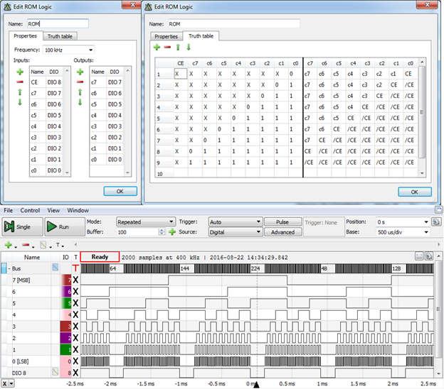
In the figure below, DIO8 is renamed CE and is used as Count Enable. DIO7…DIO0 are renamed c7…c0 and are the state/output bits of the 8-bit binary counter. Notice how X-es, signal names, and negated signal names are used in the Truth Table. The clock for the counter is 100kHz. The Truth Table was written in Excel (colored background area in sheet CounterWithCe8Bit of RomLogicTruthTables.xlsx) and copied in the appropriate tab.
Line 1 in the Truth Table (equivalent to 28=256 expanded lines) means: when LSB c0=’0’: all bits c7…c1 keep value; c0 changes to ‘1’ only if CE=’1’. All other lines cover the cases when c0=’1’.
Line 2 (equivalent to 27=128 expanded lines): means when c1=’0’ and c0=’1’: both will swap if CE=’1’ or keep their value if CE=’0’; all other bits keep their value.
All nine lines are equivalent to 29=512 expanded lines and define all possible cases (8 bit+1 Count Enable).
To verify the behavior, add a clock signal on DIO8 (Frequency=1kHz, Duty Factor=80%). As defined above, DIO8 is Count Enable for the binary counter.
In the Logic Analyzer, Add/Bus DIO7…DIO0 and Add/Signal DIO8. Run Pattern Generator and Single step Logic Analyzer. Observe the behavior of the binary counter.
Figure 8 Defining (up/middle) and verifying (down) an 8-bit binary counter with enable ROM Logic object.
6. Example: PWM modulator
In the figure below, an n-bit binary counter generates a digital sawtooth signal. The comparator drives DIOx = 1 when the sample value is greater than the counter content.
Figure 9. PWM block diagram.
The DIOx carrier frequency is:
$$f_{carrier}=f_{cnt}/2^n$$
If the n-bit sample is constant, the DIOx pin is driven with constant Duty Factor:
$$DF=(sample)/2^n$$
A 5-bit bus is created to generate the modulator n-bit samples (DIO4…DIO0). For the first experiment, the bus type is set to Number, to generate a static value between 0 and 31.
Figure 10.Pattern Generator prepared for PWM with static input.
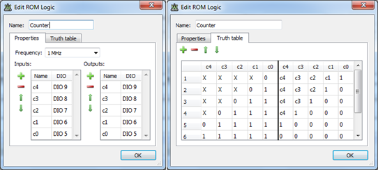
A 5-bit counter is implemented in a ROM logic object, as below, on DIO9…DIO5, renamed c4…c0. The Truth Table was written in Excel (sheet PWM in RomLogicTruthTables.xlsx) and copied in the Truth Table tab. The clock frequency is set to 1MHz.
Figure 11. 5 bit counter ROM logic.
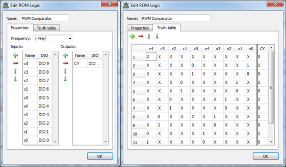
A second ROM logic (sheet PWM in RomLogicTruthTables.xlsx) compares DIO9…DIO5 = c4…c0 = “5BitCounter” with DIO4…DIO0 = s4…s0 = ”Sample”. DIO10 = CY = ”CarryOut” is High when “Sample” is higher. Notice again how higher order bits (later lines in the Truth Table) override the lower order bits (earlier lines in the Truth Table).
Figure 12. 5-by-5 bit Comparator ROM logic.
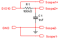
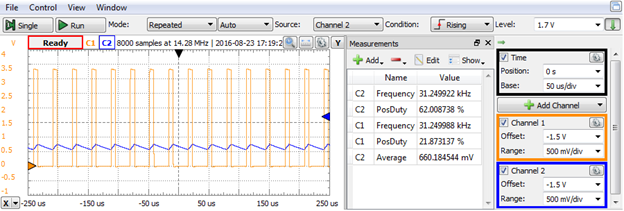
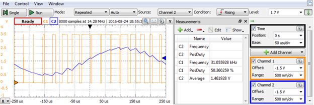
An external RC Low Pass Filter (100kΩ, 1nF) is used to build the analog signal, removing the carrier from the PWM signal. The WaveForms scope shows the PWM signal (C1) and the filtered signal (C2).
Figure 13. RC Low Pass Filter.
Notice the C1 frequency and duty factor (both on the graphical view and measurement pane):
$$f_{carrier}=f_{cnt}/2^n =1MHz/2^5 =31.25kHz;$$ $$DF=sample/2^n =7/2^5 =21.875\text%$$
Modify the sample value in the Pattern Generator and observe the effect on the scope signals.
Figure 14. Static PWM Scope capture.
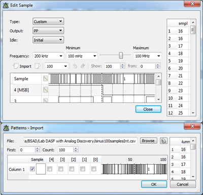
Variable n-bit sample can be used as a modulator signal. For the second experiment, set a custom 5-bit Bus 1 in the Pattern Generator, to drive a sinus signal with 100 samples per period. Generate a .csv file, with 100 values of form (sheet SinusSamples in RomLogicTruthTables.xlsx):
$$sample_i=16+int(15*sin((2∙π∙i)/100))∈[1…31]$$
Make Bus1 custom and import the .csv file. You can also copy the samples from the Excel file and paste them into the Sample column, in the Edit Custom Bus window.
Set the clock frequency to 200kHz, for a sinus frequency of:
$$ f_{modulator}=f_{sample}/(100)=200KHz/100=2kHz $$
Figure 15. Custom Bus1 for 100 samples sinus.
The scope shows the variable Duty Factor PWM signal on C1, and an analog signal on C2, approximating a sinus. The carrier frequency is constant (same as above). The Duty Factor is variable with a mean value of 50%.
Figure 16. Sinus PWM and analog signal.
7. Example: PDM modulator.
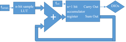
In the figure below, an n-bit accumulator is used to add the sample value over and over. The Carry Out bit is the Pulse Density Modulated (PDM) signal. The accumulator is refreshed with fcnt frequency, while samples succeed with fsample rate. Same frequencies and names are used as for PWM, for comparison.
Figure 17. PDM modulator block diagram.
For being able to switch very fast from PWM to PDM and back, a second pattern Generator instance is open from the already existing one:
Figure 18. Open a second pattern generator.
A 5-bit PDM modulator is implemented in the PDM Accumulator ROM logic object, with DIO 9…DIO5 = a4…a0 as “Accumulator”, DIO4…DIO0 = s4…s0 as “Sample” and DIO10 as “CY” which is the PDM signal (copy colored background area in sheet PDM of RomLogicTruthTables.xlsx and paste into the Truth Table).
Figure 19. Implementing a PDM in ROM logic.
The truth table is fully expanded, with 1024 lines. The left pane contains all binary values of DIO9…DIO0. The right pane contains the 5-bit + carry accumulated sum:
$$(CY,a4…a0) <= (a4…a0) + (s4…s0)$$
To compare with PWM, similar examples are used. The same external RC filter, the clock frequency of the modulator, the sinus Sample Memory and sample frequency are all the same as in the corresponding PWM experiments.
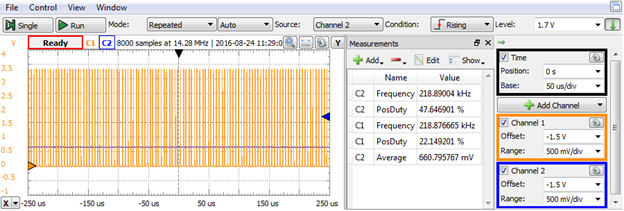
In the static experiment, the same duty factor is generated, with a much higher frequency, resulting in a much smaller ripple of the analog signal.
Figure 20. Static PDM scope capture.
In the dynamic experiment, the same sinus custom Bus1 was used, as for the PWM. The average Duty Factor is again around 50%, the frequency is variable and the average frequency is much higher compared to PWM, for the same clock frequency. The ripple of the analog signal is also much smaller.
The lowest instantaneous frequency of the PDM signal happens when the sample value is either 1LSB or 2n-1LSB, and is the same as the constant frequency of the PWM signal. For all other values of the samples, the resulting instantaneous frequency is higher, up to half of the clock frequency, when the sample value is at half of the range.
Having both instances of the Pattern generator open, is very easy to run them alternatively for easy comparison on the scope instrument. Hitting Run on one instance automatically turns the other instance in Busy state.
Figure 21. Sinus PDM and analog signal.
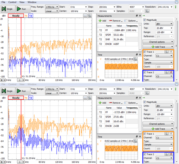
The spectrum analyzer instrument is used to analyze data in the frequency domain. The two traces correspond to the two scope channels in the experiments above. In the spectral view, a cursor is set at fcarrier. Some parameters of the modulated and analog signals are shown in the measurements window.
The carrier fundamental and harmonics are significant for PWM, while PDM spread those components more uniformly in the spectrum.
The measurements have much better values for SFDR, SNR, SINAD and ENOB in the case of PDM.
Figure 22. Spectral comparison

