Getting Started with Vivado
For the most up to date version of this guide, please visit Getting Started with Vivado for Hardware-Only Designs.
Introduction
The goal of this guide is to familiarize the reader with the Vivado tools by building the “Hello World” of hardware, blinking an LED.
Prerequisites
Hardware
- Digilent FPGA System Board
- MicroUSB Programming Cable
Software
- Xilinx Vivado 2018.2 and Digilent Board Files
- Other versions of Vivado may work, but functionality is not guaranteed
- See the Installing Vivado and Digilent Board Files tutorial for more information.
1. Starting Vivado
Windows
Open Vivado via the start menu or desktop shortcut created during the installation process.
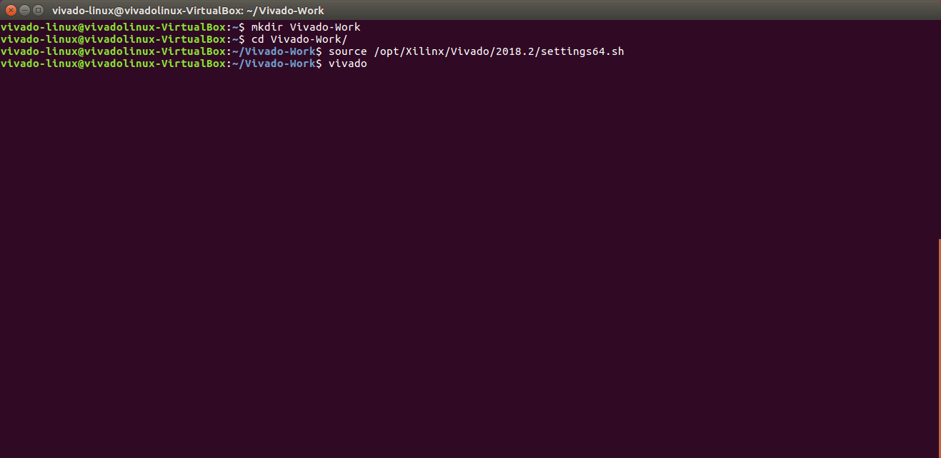
Linux
Open a terminal, cd into a working directory that can be cluttered with temporary Vivado files and logs, then run the following two commands:
source <install_path>/Vivado/<version>/settings64.sh
vivado
For a default installation of Vivado, the install path will be “C:/Xilinx/” on Windows, and “/opt/Xilinx/” on Linux.
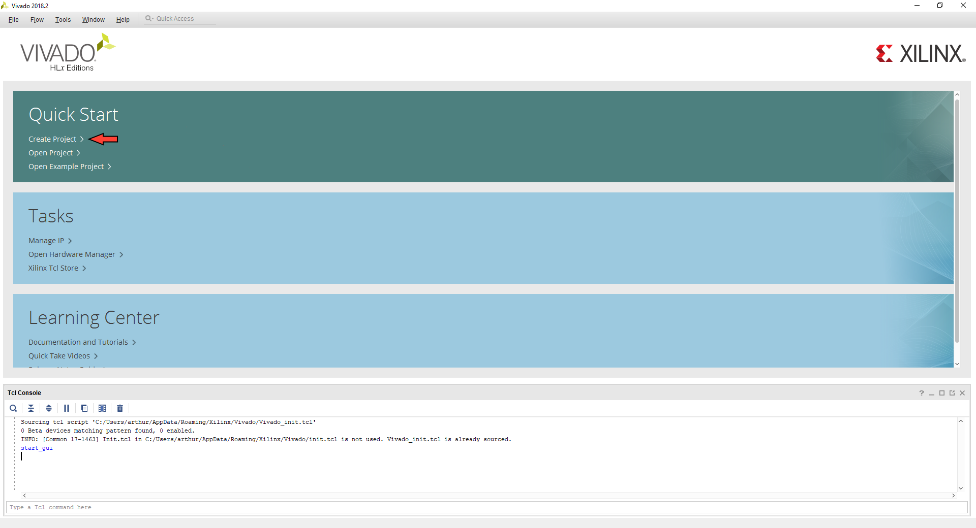
2. The Start Page
This is the screen Vivado's start-up screen. The different options available are described below using the image as a guide.
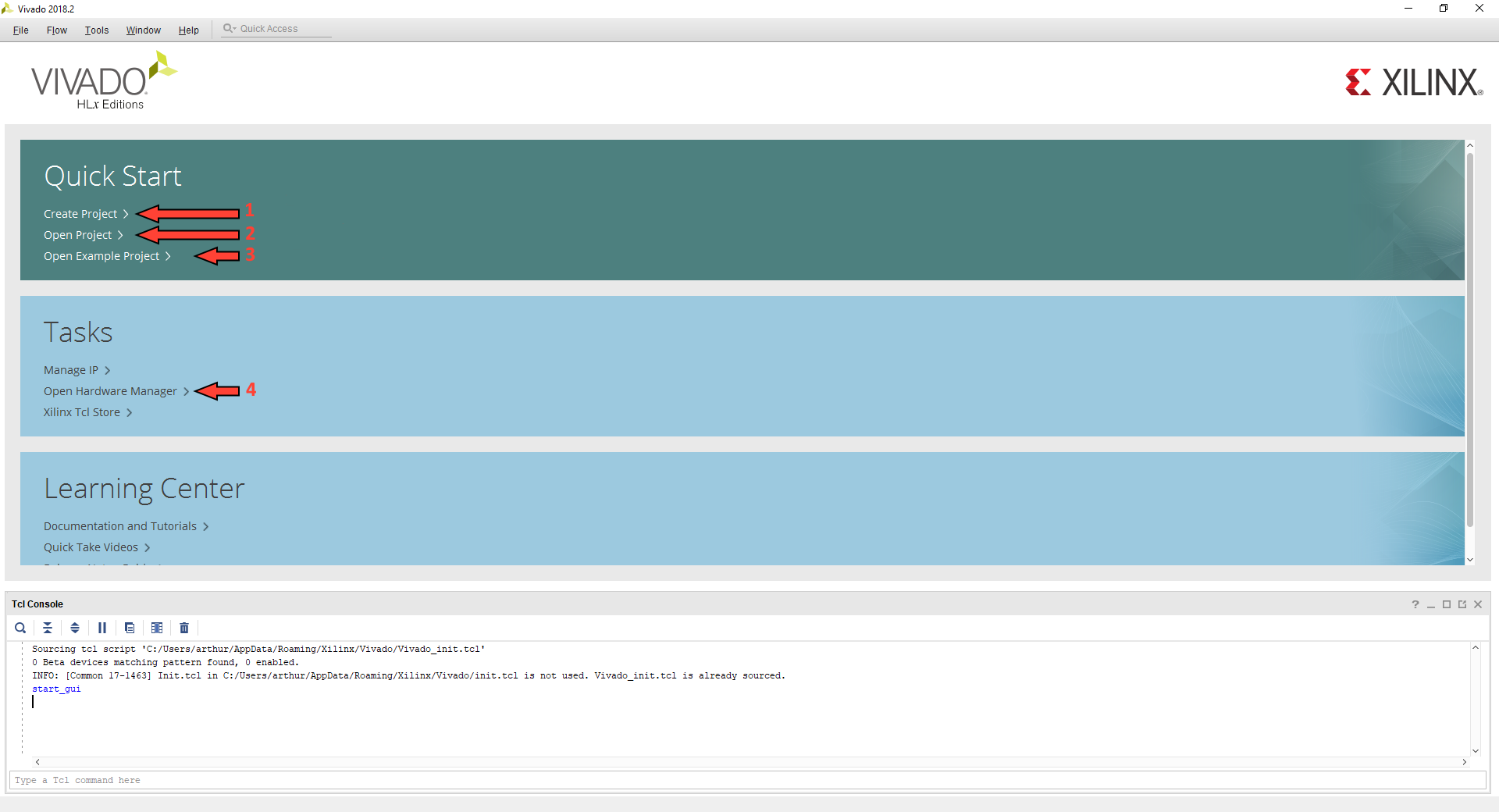
- Create New Project: This button will open the New Project wizard. This wizard steps the user through creating a new project. The wizard is stepped through in section 3.
- Open Project: This button will open a file browser. Navigate to the desired Xilinx Project (.xpr) file and click Open to open the project in Vivado.
- Open Example Project: This will guide the user through creating a new project based on an example project. These projects will not work on all devices. Many Digilent example projects are instead released on Github, and linked to through the target FPGA System Board's Resource Center, which can be found through the list of List of Digilent FPGA System Boards.
- Open Hardware Manager: This will open the Hardware Manager without an associated project. If connecting to and programming a device is all that the user wants to do, then this is the button to use.
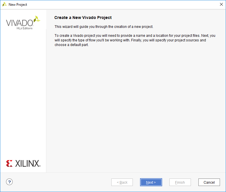
3. Creating a New Project
3.1
From the start page, click the Create New Project button to start the New Project Wizard.
3.2
The text in this dialog describes the steps that will be taken to create a project. Click Next to continue.
3.3
The first page is used to set the name of the project. Vivado will use this name when generating its folder structure.
Important
Do NOT use spaces in the project name or location path. This will cause problems with Vivado. Instead use an underscore, a dash, or CamelCase.
Click Next to continue.

3.4
Now that the project has a name and a place to save its files we need to select the type of project we will be creating. Select RTL Project and make sure to check the Do not specify sources at this time box. Source files will be added and created after the project has been created. Advanced users may use the other options on this screen, but they will not be covered in this guide.
Click Next to continue.

3.5
Important
If the target board does not appear in this list, then Digilent's board files haven't yet been installed. If this is the case, revisit the prerequisites section of this guide, then close Vivado and start again from the beginning.
Now it is time to choose the target device. Click the Boards tab at the top of the dialog, then select the target board from the list.
Click Next to continue.

3.6
The next section gives a summary of the options selected throughout the wizard. Verify that the information looks correct and click Finish.

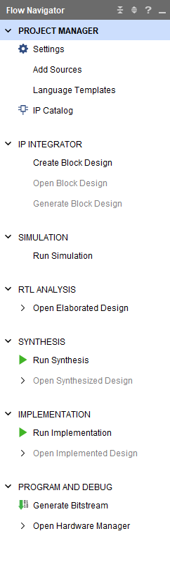
4. The Flow Navigator
The Flow Navigator is the most important pane of the main Vivado window to know. It is how a user navigates between different Vivado tools.
The Navigator is broken into seven sections:
- Project Manager: Allows for quick access to project settings, adding sources, language templates, and the IP catalog.
- IP Integrator: Tools for creating complex designs in a graphical user interface, rather than by writing large source files.
- Simulation: Allows a developer to verify the output of their deisgn prior to programming the target device.
- RTL Analysis: Lets the developer see how the tools are interpreting their code.
- Synthesis: Gives access to Synthesis settings and post-synthesis reports.
- Implementation: Gives access to Implementation settings and post-implementation reports.
- Program and Debug: Gives access to settings for bitstream generation and tools to program FPGAs.
5. The Project Manager
This tool is where most development will occur and is the initial tool open after creating a new project.
The Project Manager consists of four panes, Sources, Properties, Results, and the Workspace, described below.
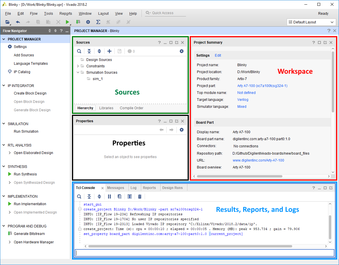
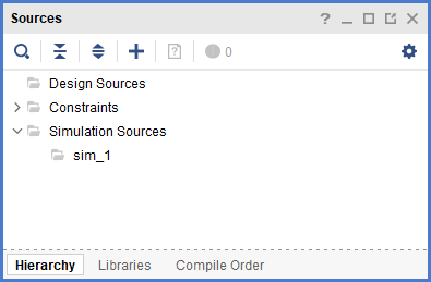
Sources Pane
The Sources pane contains the project hierarchy and is used for opening up files. The folder structure is organized such that the HDL files are kept under the Design Sources folder, constraints are kept under the Constraints folder, and simulation files are kept under the Simulation Sources folder. Files can be opened in the Workspace by double-clicking on the corresponding entry in the Sources pane. Sources can also be added by either right clicking the folder to add the file to and selecting Add Sources or by clicking the Add Sources button ( ).
).
Properties Pane
The Properties pane allows for viewing and editing of file properties. When a file is selected in the Sources pane its properties are shown in here. This pane can usually be ignored.

Results, Reports, and Logs
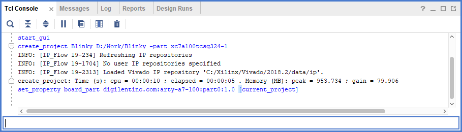
TCL Console Tab
The Tcl Console is a tool that allows running commands directly without the use of the main graphical user interface.
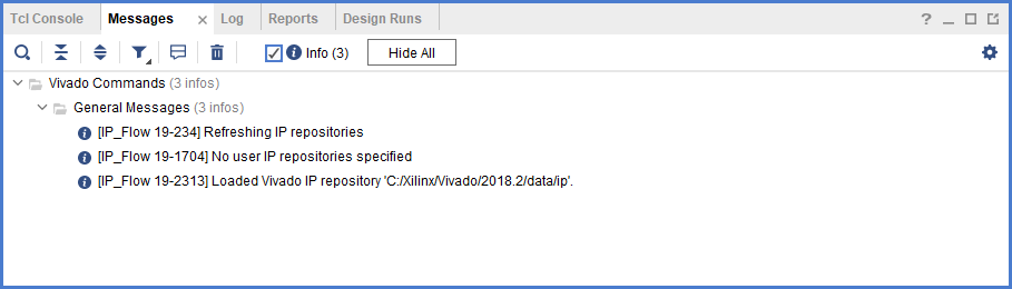
Messages Tab
The Messages tab displays warnings (critical or otherwise) and errors that may occur during the process of building a project. If anything goes wrong while designing and building a project, check the Messages first. Solutions for many errors and warning can be found by right clicking on the message and selecting “Search for Answer Record”.
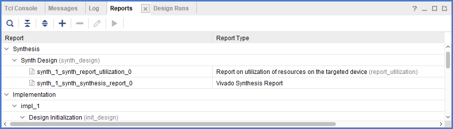
Reports Tab
The Reports tool is useful for quickly jumping to any one of the many reports that Vivado generates on a design. These include power, timing, and utilization reports just to name a few.
Log Tab
The Log displays the output from the latest Synthesis, Implementation, and Simulation runs. Digging into this is usually not necessary as the reports and messages view store the information in the log in a more readable format.

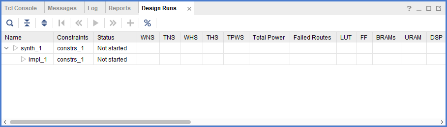
Design Runs Tab
The last tool is the Design Runs. Using this tool, run settings can be edited and new runs can be created. This tool is useful when targeting multiple devices with the same design.
Workspace Pane
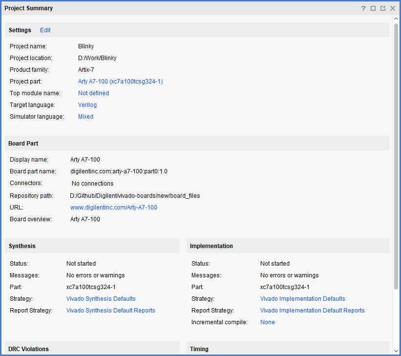
The most important pane in the Project Manager is the Workspace. The Workspace is where reports are opened for viewing and source files are opened for editing. Initially the Workspace displays the Project Summary which show some basic information from some of the reports.
6. Adding a Constraint File
In order to connect the inputs and outputs of an HDL design with the physical pins of the FPGA, a constraint file needs to be added or created. Digilent has produced a Xilinx Design Constraint (XDC) file for each board. Download the ZIP Archive containing each of these master XDC files, and extract it in a memorable location.
6.1
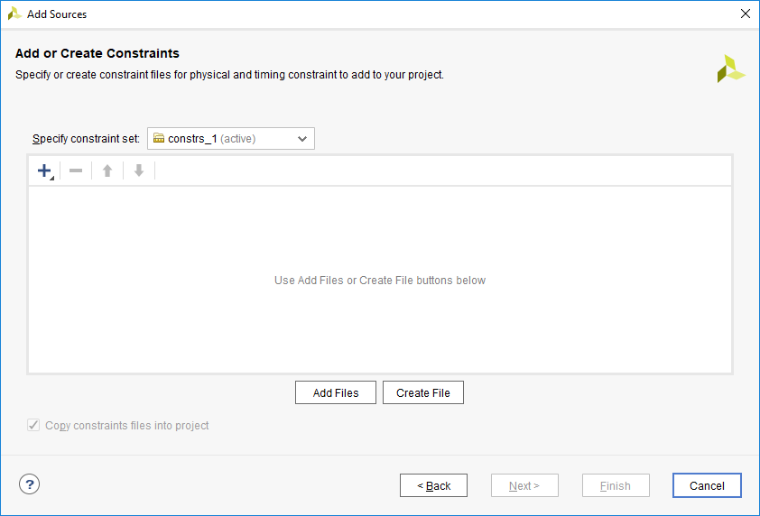
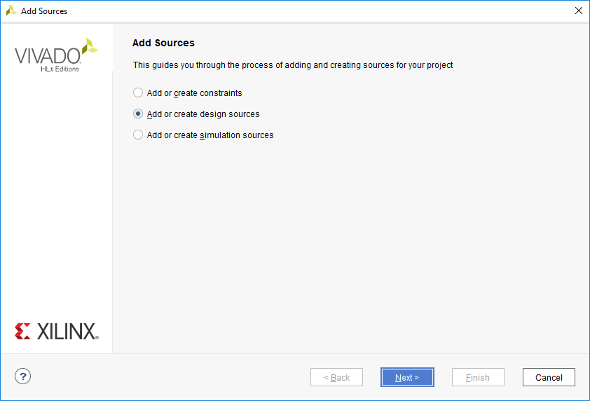
In the Project Manager section of the Flow Navigator, click the  button. In the wizard that pops up, select Add or create constraints then click Next.

6.2
At this stage, Vivado provides a list of all of the constraint files that will be added or created when we click Finish. Currently this list is empty, this will change when files have been added or created. A constraint file will not be created from scratch in this guide, so click Add Files.
6.3
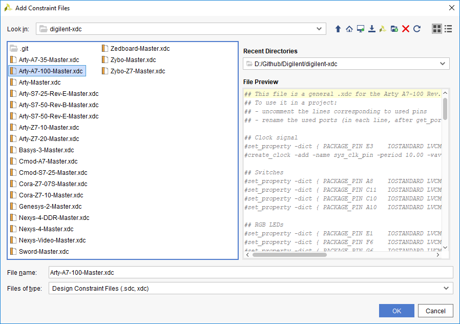
Find the directory the “digilent-xdc-master.zip” archive was extracted into, then click on the file for the target FPGA system board.
Click OK to continue.
6.4
Make sure that the selected XDC file has been added into the list of sources. Make sure that the “Copy constraint files into project” box is checked, so that the original file will be left alone so that it can be used in other projects. Click Finish.

6.5
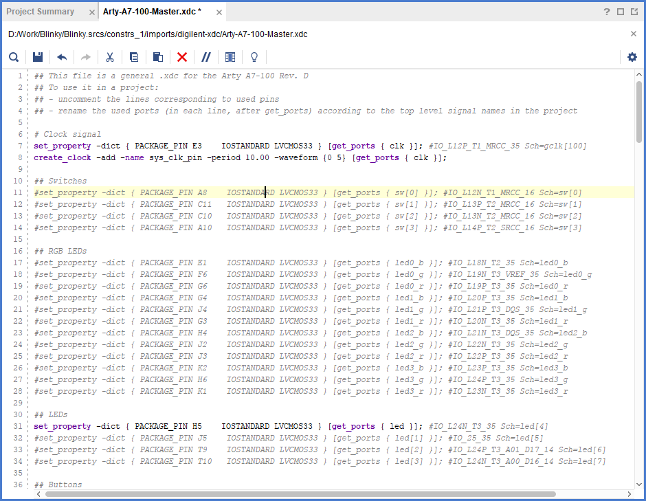
In the Sources pane of the Project Manager, expand the Constraints folder, then double click on the XDC file that was just added. Each of Digilent's XDC files contains constraints for each of the commonly used peripherals on their respective boards. For this demo, constraining the default system clock and a single led is required.
Find and uncomment the lines that call get_ports on the names led[0] and clk by removing the '#' symbol at the beginning of the line. On some boards the clock port will consist of two different ports, clk_p and clk_n. The clock port is occasionally named something like sysclk, but should appear at the top of the XDC file. Uncomment the create_clock line that follows the clock port/s definition as well.
Tip
A board using clk_p/clk_n pins means that the input clock that uses differential logic. Check out the Wikipedia article on low-voltage differential signalling for more information.
Change the name inside of the get_ports call to 'led' from 'led[0]'. Do the same for the clock if it is something other than 'clk' or 'clk_p' and 'clk_n'.
7. Creating a Verilog Source File
7.1
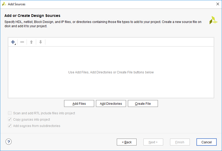
In the Project Manager section of the Flow Navigator, click the button again. Select Add or create design sources then click Next.
7.2
As before, at this stage, a list is provided of all of the source files that will be added or created when Finish is clicked. Instead of clicking Add Files, click Create File.
Tip
It is also possible to add existing source files in the same way as the the constraint file was added above.
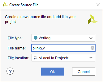
7.3
When prompted to select a File type, File name, and File location, make sure to pick Verilog and <Local to project> for the type and location. Give the file a name ending in '.v'.
Important
Do NOT use spaces in file names. This will cause problems with Vivado. Instead use an underscore, a dash, or CamelCase.
Click OK to continue.
7.4
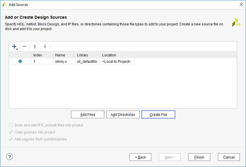
Make sure that the new Verilog source file has been added into the list of sources, then click Finish.
7.5
Unlike when the constraint file was added, at this point a Define Module dialog will pop up. The Verilog module can be renamed using the Module name field, but this is unnecessary in this instance. The Verilog module's clock and led ports need to be defined. Clicking the Add ( ) button will add an empty slot for a port to the I/O Port Definitions list.
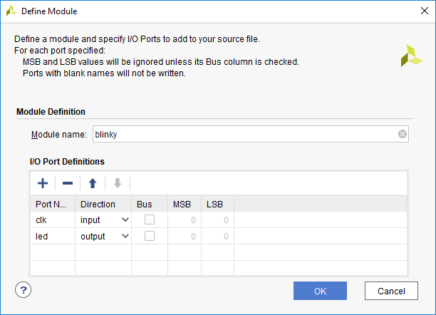
There are five fields to define for each of the module's I/O ports:
- Port Name: This field defines the name of the port and needs to match one of the names used in the XDC file.
- Direction: This drop-down menu can be set to input, output, or inout, defining the direction that signals propagate through the port, with respect to the Verilog module. Outputs are the signals that the module will control.
- Bus: This box can be checked or not; when checked, the port will consist of multiple single bit signals, grouped into a single bus.
- MSB: This field sets the index of the most significant bit of the port, if it is a bus. This option is grayed out for single-bit ports.
- LSB: This field sets the index of the least significant bit of the port, if it is a bus. This option is grayed out for single-bit ports.
Tip
When defining a module which will be instantiated in another module, which is beyond the scope of this guide, be aware that the port names should not be declared in the XDC, this is only done for the 'top' module.
If the target board uses differential clocking, add two single-bit input ports with the same names as the positive and negative clock ports that were uncommented in the XDC file. Otherwise, add a single single-bit input port with the same name as the clock port that was uncommented in the XDC file.
Add a single-bit output port with the same name as the LED port that was uncommented in the XDC file.
Once these two or three ports have been added, click OK to continue.
7.6
At this point, the new source file will be added to the Design Sources folder in the Sources pane of the Project Manager. Expand this folder and double click on the file to open it.
Next, some Verilog code needs to be written to define how the design will actually behave.

Between the ');' that comes after the module's port list and the 'endmodule' statement, add the following code:
reg [24:0] count = 0;

assign led = count[24];

always @ (posedge(clk)) count <= count + 1;
If the target board is differentially clocked, add the following lines of code after ');' and before the 'reg [24:0] count = 0;' line:
wire clk;

IBUFGDS clk_inst (
    .O(clk),
    .I(clk_p),
    .IB(clk_n)
);
It should be noted that the rate at which the clock will blink will differ depending on the board used. System clocks on different Digilent boards run at a number of different rates, depending on the needs of the board. The system clock period in nanoseconds can be found on the create_clock line of the XDC file.
8. Synthesis, Implementation, and Bitstream Generation
In order to create a file that can be used to program the target board, each stage of the “compilation pipeline” needs to be run.
This starts with Synthesis. Synthesis turns HDL files into a transistor level description based on timing and I/O constraints. To run Synthesis click either  in the toolbar or
  in the Flow Navigator. The output of Synthesis is then passed to Implementation.
Implementation has several steps. The steps that are always run are Opt Design (Optimize the design to fit on the target FPGA), Place Design (Lay out the design in the target FPGA fabric), and Route Design (Route signals through the fabric). To run Implementation click either  in the toolbar or
  in the Flow Navigator. This output is then passed on to the Bitstream Generator.
The Bitstream Generator generates the final outputs needed for programming the FPGA. To run Bitstream Generation click either  in the toolbar or
  in the Flow Navigator. With no settings changed, the generator will create a '.bit' file, which can be used to program the design onto the target FPGA system board.
Bitstream Generation Completed Pop-Up
Once the bitstream has been generated, a pop-up will appear asking what Vivado should do next. The options in this pop-up allow the user to do several different things:
- Open Implemented Design takes the user to a tool where they can view how the project will be programmed into the fabric of the target FPGA chip.
- View Reports takes the user to a list of many different reports and statistics about how the project was laid out, including information about how fast the design can potentially be run, and how much of the FPGA will be used to run the design.
- Open Hardware Manager takes the user to a tool that can be used to program the generated bitstream onto a connected FPGA board.
- Generate Memory Configuration File lets the user create a file that can be used to program a non-volatile memory part on an FPGA system board, so that the FPGA can be automatically programmed each time that the board is powered on.
For the purposes of this guide, select Open Hardware Manager, then click OK.

9. The Hardware Manager
First, plug the target FPGA system board into the computer running Vivado using a MicroUSB cable capable of transferring data. With the board plugged in, it needs to be connected to the Vivado Hardware Server. There are two ways to do this through the Vivado Hardware Manager:
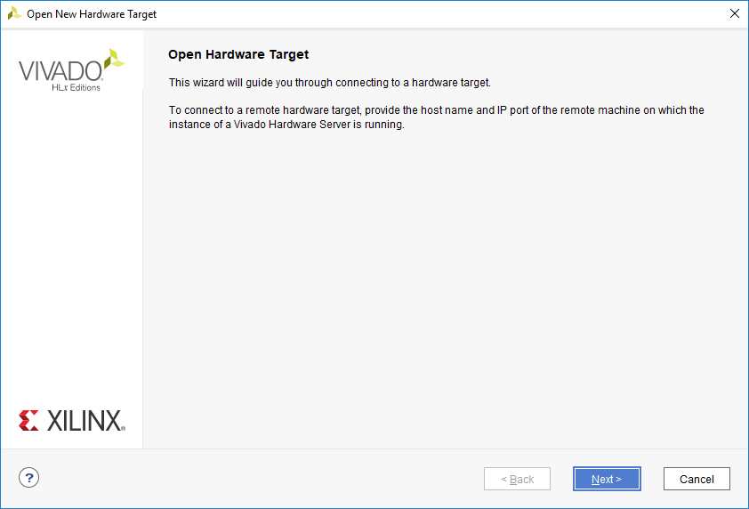
9.1(A) Open New Hardware Target
9.1(A).1
The first method is to manually open the target. This is required if the hardware is connected to a computer other than the one running Vivado (outside of the scope of this guide). To get to the Open Hardware Target wizard either:
- Open the Hardware Manager and click the
 link in the green banner at the top of the screen.
 - Or click the
 button in the Flow Navigator under
  .
.
From the drop-down that opens from either button, click  .
.
Once the wizard opens, click Next.
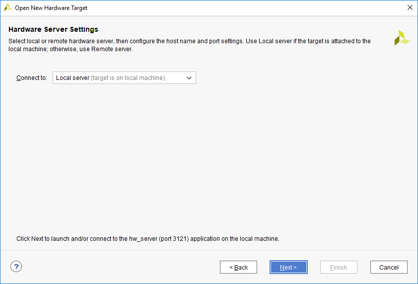
9.1(A).2
The next screen asks if the hardware server is local or remote. If the board is connected to the host computer choose local, if it is connected to another machine choose remote and fill in the Host Name and Port fields.\
Click Next to continue.
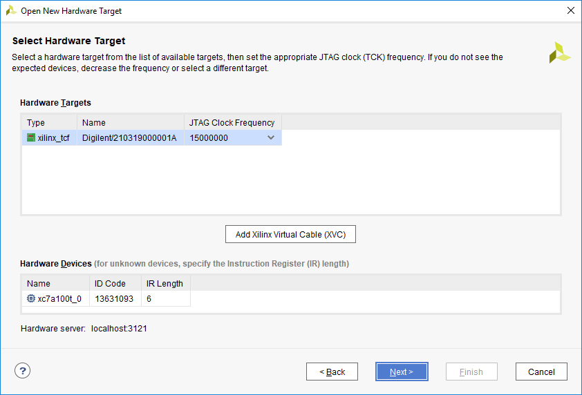
9.1(A).3
This screen gives a list of devices connected to the hardware server. If there is only one connected it should be the only device shown. If there are multiple connected devices, determine the serial number of the device to connect to and find it in the list.
Click Next to continue.
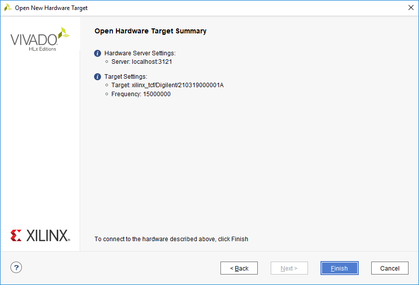
9.1(A).4
The final screen shows a summary of the options selected in the wizard. Verify the information and click Finish. The board is now connected to the hardware manager.
9.1(B) Auto-Connect
The second method is to automatically open the target. To get to the  button either:
- Open the Hardware Manager and click the link in the green banner at the top of the window
- Or click the button in the Flow Navigator under .
From the drop-down that opens from either button click . Vivado will attempt to find a hardware server running on the local machine and will connect to the device from the server.
9.2 Programming
To program the device with the bit file generated earlier, either click the  link in the green banner at the top of the window or click the
  button in the Flow Navigator under . From the drop-down that opens, select the device to program (Example:
  ) and the following window will open:
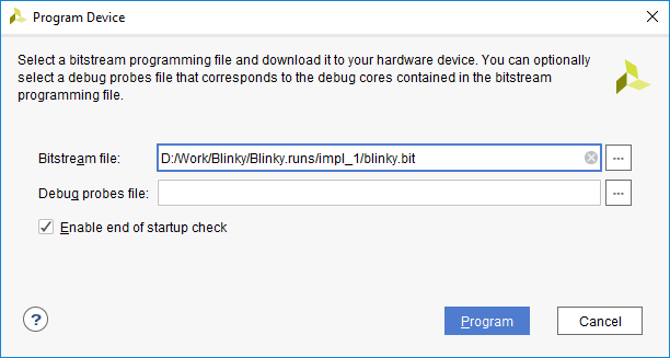
The Bitstream File field should be automatically filled in with the bit file generated earlier. If not, click the  button at the right end of the field and navigate to
<Project Directory>/<Project Name>.runs/impl_1/ and select the bit file (Example:  ). Now click Program. This will connect to the board, clear the current configuration, and program using the new bit file.
10. Finished!
One of the LEDs on the programmed board will now be blinking! The rate at which the LED blinks depends on the speed of the clock used by the FPGA. Given that the counter created in the Verilog source file takes 225 clock cycles to roll over, for a 100MHz clock, the LED will blink three times per second. One possible next step to learn some more about verilog would be to try to modify the Verilog source file so that the LED blinks only once per second. There are many good resources online to learn more about Verilog and other hardware description languages, far more than could be listed here.
Be sure to visit the resource center for the FPGA board used for more tutorials and demo projects. A link to each resource center can be found here.