Getting Started with Vivado IP Integrator
For the most up to date version of this guide, please visit Getting Started with Vivado and Vitis for Baremetal Software Projects.

Prerequisites
- A Digilent FPGA Board.
- Vivado installed. See this tutorial to install Vivado.
- This guide uses version 2016.4, other versions can be used, but there may be differences.
- Digilent Board Files installed to handle selecting complicated configuration settings. See this tutorial.
- Basic familiarity with Vivado. See this tutorial.
Introduction
This guide will explain the use of most of the major features of the IP Integrator design flow for a Digilent FPGA board. At the end of the demo, a simple design that receives data from on-board switches and controls LEDs will have been created.
1. Create a New IPI Project
1.1
With Vivado freshly opened, click Create New Project.

1.2
The first page of this wizard summarizes the steps involved in creating a project. Click Next.

1.3
The first step is to set the name of the project. Vivado will use this name when generating its folder structure.
Important
Do NOT use spaces in the project name or location path. This will cause problems with Vivado. Instead use an underscore, a dash, or CamelCase.
Click Next to continue.

1.4
At the Select Project Type screen, choose RTL Project and check the Do not specify sources at this time box. Advanced users may want to use the other options on this screen, but they will not be covered in this guide.
Click Next to continue.

1.5
This screen selects the part targeted by the project. If Digilent's Board Files haven't yet been installed, return to the prerequisites section of this guide and follow the link to that tutorial, Vivado will then need to be restarted to load these files properly. Select the Boards tab, then find and select the target board from the list. Click Next.

1.6
This screen summarizes selections chosen in the previous screens. Click Next to finish opening the new project.

2. Open the IP Integrator
2.1
A more complete run-down of the standard Vivado work-flow can be found in Digilent's Getting Started with Vivado tutorial. This guide will be exclusively using the IP Integrator tool, which can be opened from the Flow Navigator on the right side of the window. Expand the IP Integrator tab and select Create Block Design.

2.2
In the dialog box, give the block design a name. The directory location is where the block design will be stored, this can be changed, but it is recommended to leave it as <Local to Project>. Make sure that Specify source set is set to Design Sources.
Important
Do NOT use spaces in the block design name or directory path. This will cause problems with Vivado. Instead use an underscore, a dash, or CamelCase.
Click OK to create the block design and open IPI.

3. IP Integrator Tools
The project described in this guide consists of two major segments, logic implemented in an FPGA and a processor. Depending on the target board, the processor may be implemented within the FPGA fabric, rather than being a distinct hardware component, but for the most part, this is irrelevant.
The communications protocol used to move data between peripherals implemented on the FPGA and processor is called AXI (Advanced eXtensible Interface). Each AXI peripheral implemented onto the FPGA will be assigned an area of the Zynq's memory space that will be used to address each of its control registers. Adding a simple AXI interface to a design will require the addition of two new blocks, the AXI Interconnect, which defines how the AXI signals are routed, and the reset controller, which will generate the resets of each AXI block and the interface.
Much of basic block design consists of connecting different AXI peripherals to a processor and using them to read from and write to input and output ports.
With this context out of the way, many of the tools that can be used to create a design in Vivado IPI will be described.
3.1
The Sources tab, highlighted in orange in the image to the right, contains several sub-tabs, of these, Hierarchy and IP Sources are the most immediately useful.
The Hierarchy sub-tab shows the set of sources that exist in the project. These are split up into three groups, Design Sources contains the block design, and beneath that, sources for all of the IP cores or other files that are included in the block design. The Constraints sub-tab contains Xilinx Design Constraint (XDC) files that have been added to the project. XDC files can be used to constrain ports that have been omitted from the board file.
The IP Sources sub-tab shows the files generated when a new IP core has been added to the block design. Some annoying errors can be solved by right clicking on the block design in this screen and selecting Reset Output Products followed by Generate Output Products.

3.2
When the Design tab is selected, a list of all input and output ports, IP core ports, and connections between IP cores is shown. Selecting an entry in this list will highlight that object in the block design diagram.

3.3
The Signals tab allows the user to view lists of all clock and reset signals in the block design. As before, selecting an entry in either of these lists will highlight that signal in the block design diagram. This tool can be useful for figuring out where data crosses clock domains in a more complicated design.

3.4
The Board tab displays all of the external connections that Digilent has provided as part of the board file selected as part of creating the project. This tool makes connecting these ports to a design extremely straightforward. The process of connecting one of these ports will be gone through later in this guide.

3.5
The Properties pane, found below the tabbed pane described above, shows the properties of the currently selected object. This pane is typically used to quickly view the clock frequency of a selected clock pin, or to change the name of an IP core or port.

3.6
Most of the upper right of the Vivado window is taken up by the Diagram pane. This pane displays a graphical rendition of the current block design. Many of the buttons in the toolbar to the left side of this pane will be described in Step 4 of this guide.

3.7
The Address Editor tab, contained in the same pane as the Diagram, describes the memory addresses that the processor can find each installed AXI peripheral at. Changing values in this pane is not recommended, except for advanced users. Errors in the block design validation process that refer to unmapped peripherals can be solved by right clicking anywhere in this pane and selecting Auto-Assign Address.

3.8
The first tab of the pane at the bottom of the window is the TCL Console. This tool displays the scripted commands that Vivado is running whenever a change is made in the graphical interface. Scripts can be created to be run using this tool through the use of the 'source' command.

3.9
The Messages tab displays Error, Warning, Info, and Status messages created when Vivado takes different actions. These messages can also be found in the TCL Console but are presented in a relatively easy to navigate format.

3.10
The Reports tab contains a list of different reports that Vivado generates as part of the process of generating a bitstream.

3.11
By selecting Tools → Reports → Report IP Status in the toolbar at the top of the Vivado window, another tab will be added to the bottom-most pane - though this will not do anything until an IP is added to the design. This IP Status tab displays the versions and target devices of each IP core added to the project. If an IP is not Up-to-date, clicking the Upgrade All button will reload the IP with the most recent version, or make any updates needed to make the IP work in the version of Vivado being used.

3.12
The toolbar at the left of the Diagram pane has a large number of buttons that all do different things.
- Block Design Options (
 ) lets the user change what is displayed and how in the diagram window.
 - Zoom In (
 ) zooms in the view, while maintaining the current center position.
 - Zoom Out (
 ) zooms out the view, while maintaining the current center position.
 - Zoom Fit (
 ) zooms the view so that all blocks in the current design are shown on screen.
 - Select Area (
 ) selects every block in a drawn rectangle, useful for moving groups of blocks at once.
 - Fit Selection (
 ) zooms the view to center on the currently selected block/s.
 - Search (
 ) launches a search through the ports and blocks in the current design.
 - Add IP (
 ) launches a search dialog to add a new IP block to the design. More on this later.
 - Make External (
 ) creates an input or output port for the currently selected pin. This is useful when constraining ports with an XDC file, rather than the Digilent board file.
 - Customize Block (
 ) launches the customization dialog for the currently selected block. More on this later.
 - Validate Design (
 ) tells Vivado to look for mistakes in the block design, required before generating a bitstream. More on this later.
 - IP Settings (
 ) opens the project settings dialog at the IP settings page. Useful for including non-standard IP repositories.
 - Regenerate Layout (
 ) tells Vivado to visually clean up the block design by moving IP blocks and rerouting signals.
 - Optimize Routing (
 ) tells Vivado to visually clean up the block design by only rerouting signals.
 - Show Interface Connections Only (
 ) hides clock and reset signals, only useful for highly complex designs.


Additionally, changes to the design can be made by interacting directly with the Diagram pane's graphical interface. Objects can be moved by clicking and dragging them. Connections can be made by hovering over a port until the pencil cursor ( ) appears, then drawing a line to another port, pin, or wire.
With a general understanding of the actions that can be taken in the IPI, a design can now be created.
4. Create a Simple Block Design
4.1
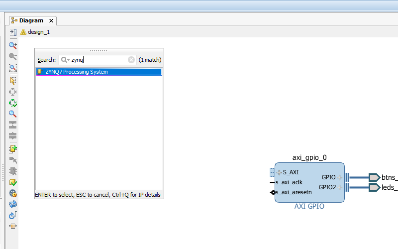
Right click on Push Buttons in the board tab, then select connect component. In the dialog that pops up, select GPIO under Create new IP → AXI GPIO.
Important.
Make sure to connect the button component to GPIO specifically, not GPIO2. The C source code provided later assumes this to be the case.
Click OK to continue.

4.2
Right click on LEDs in the board tab, then select connect component. In the dialog that pops up, select GPIO2 under Connect to existing IP → axi_gpio_0. Click OK to continue.
If there is an entry for RGB LEDs in the board tab, connect that component to another new AXI GPIO controller.

The remainder of this section branches depending on the board the project is being designed for. If the target board uses a Zynq chip, open the Zynq drop-down below, otherwise, open the Microblaze drop-down below.
- Zynq
-
4.3
Click the Add IP button (
) and search for 'Zynq'. Select Zynq7 Processing System from the list of results and press Enter on the keyboard to continue.
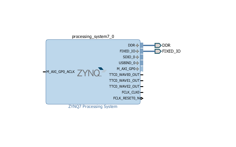
Doing this adds a Zynq processor to the block design. A Zynq chip contains both FPGA fabric and a hardware processor. This block represents the processor, as well as other hardware components not part of the FPGA.
4.4
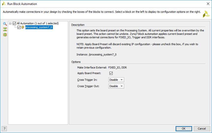
Click Run Block Automation in the green bar at the top of the screen. This will launch a dialog that allows initial configuration of the Zynq block.
In the Run Block Automation dialog, make sure that Apply Board preset under All Automation in the panel to the left is checked.
There are a number of different options available. For the purposes of this guide, set these options to the value found in parentheses below.
- Make Interfaces External (Not Configurable): This field shows the different interface ports on the Zynq block that will be automatically connected out of the design.
- FIXED IO represents connections to hardware peripherals in the programmable system side of the Zynq chip. This includes a UART connection to a host computer.
- DDR represents the connection to the external DDR memory on the board.
Click OK to continue.
4.5
Additional changes can be made to the Zynq block's configuration, depending on the requirements of the project. For example, the Zynq block can be used to generate new clocks of different frequencies. Select the Zynq block by clicking on it and then clicking the Customize Block (
) button, or by double-clicking on the Zynq block.
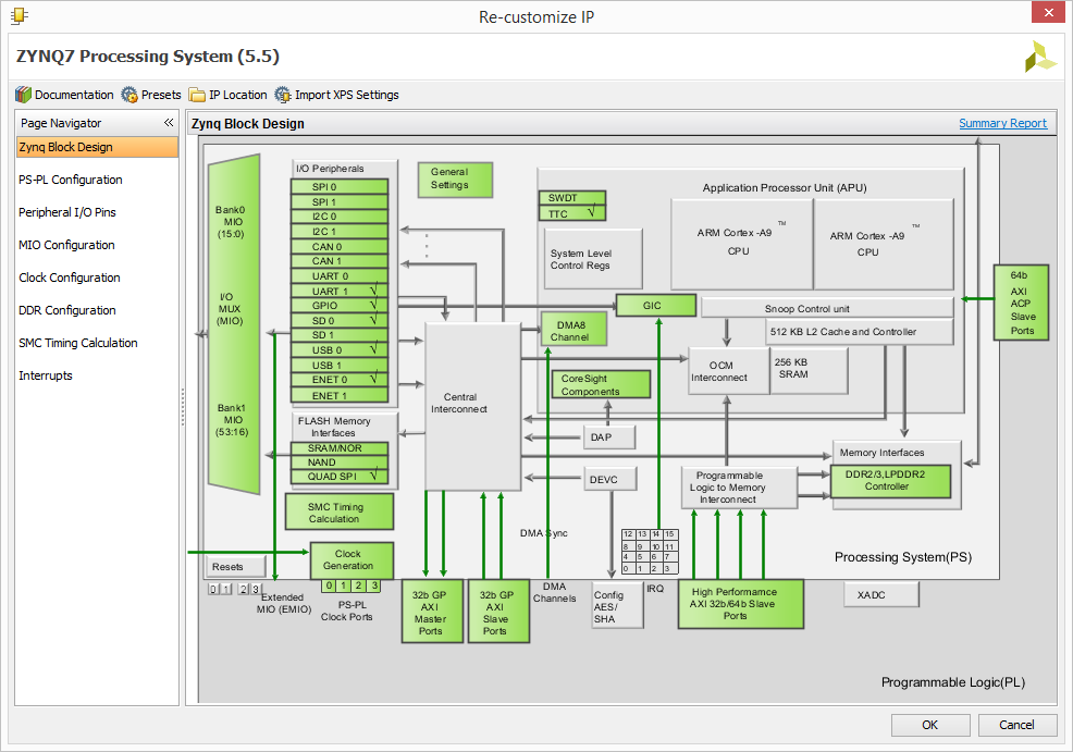
The Zynq Configuration drop-down below walks through each of the screens in the Zynq's Re-Customize IP dialog.
- Zynq Configuration
-
4.5.1
The page that opens when the Zynq block is re-customized is called Zynq Block Design. This page displays the hardware used by the Zynq chip. Note the I/O Peripherals block, the check-marks display what peripherals are currently enabled. All of the information shown in this screen is available in lists in the other pages.
4.5.3
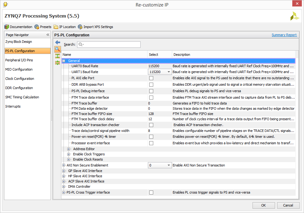
The PS-PL Configuration page allows the user to customize how the processor will communicate with the FPGA. There are several settings of particular note here.
- The UART baud rate settings found in the General drop-down are used to change the baud rate that the Zynq communicates with a computer serial port at.
- GP/HP Slave AXI Interfaces (General Purpose / High Performance) are used when an AXI peripheral requires control over a memory interface, this can be seen in Digilent's HDMI and Audio DMA demo projects.
4.5.4
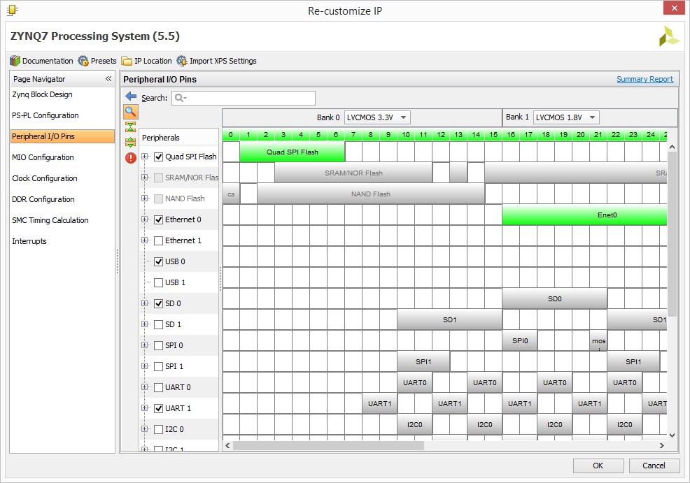
The Peripheral I/O Pins page allows the user to enable or disable a large number of different hardware peripherals that cannot be controlled directly from the FPGA. As an example, enabling GPIO MIO allows the user to control LED 4 (LD4/MIO7) on the Zybo board.
4.5.5
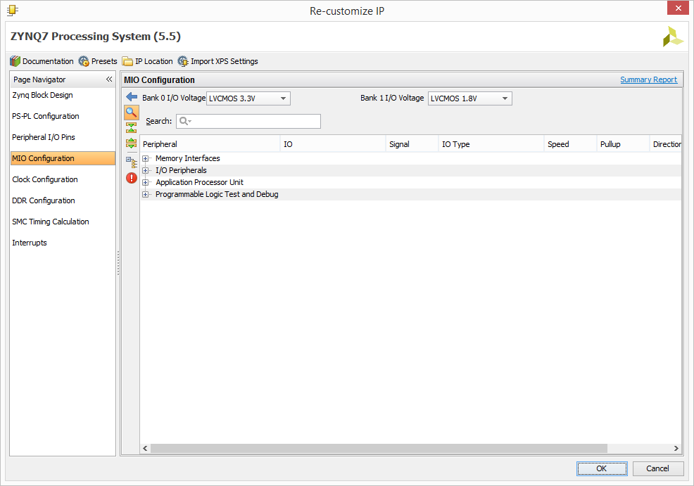
The MIO Configuration page shares much of its information with Peripheral I/O Pins, and allows the user to view this in a list, rather than the graphical table format.
4.5.6
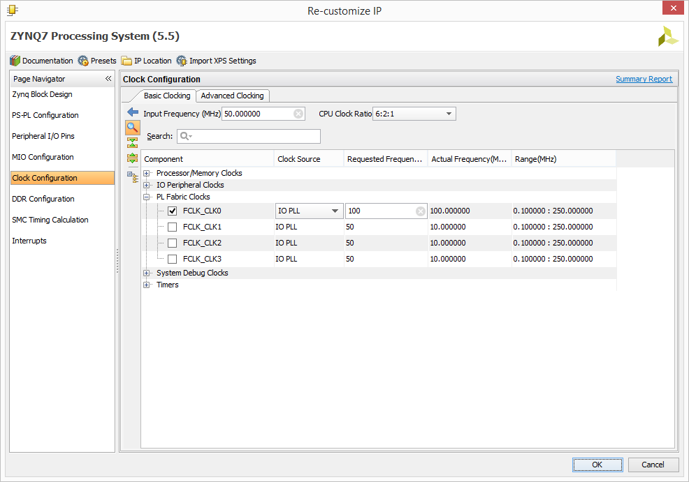
The Clock Configuration page contains important settings that allow the user to provide additional clocks at different speeds to the FPGA, as well as tweaking the clock frequencies of several IO Peripherals. Take note of the PL Fabric Clocks drop-down, checking a box for one of FCLK_CLK1-3 will provide an additional clock output from the Zynq block, at or near the provided Requested Frequency.
4.5.7
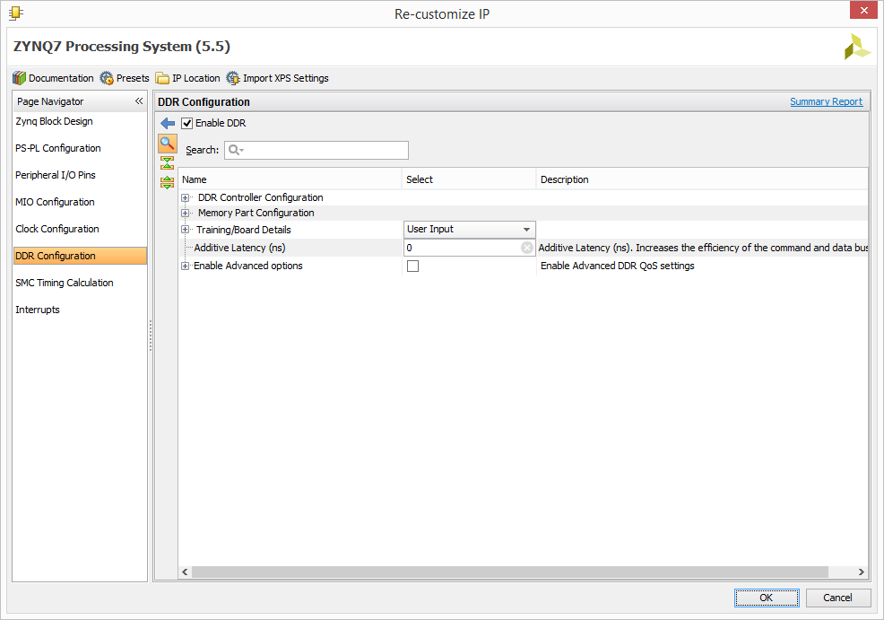
The DDR Configuration page contains a large number of settings about the DDR chip connected to the Zynq chip. This page alone is the reason to use the board preset brought in from Digilent's board file. Changing these settings is not recommended.
4.5.8
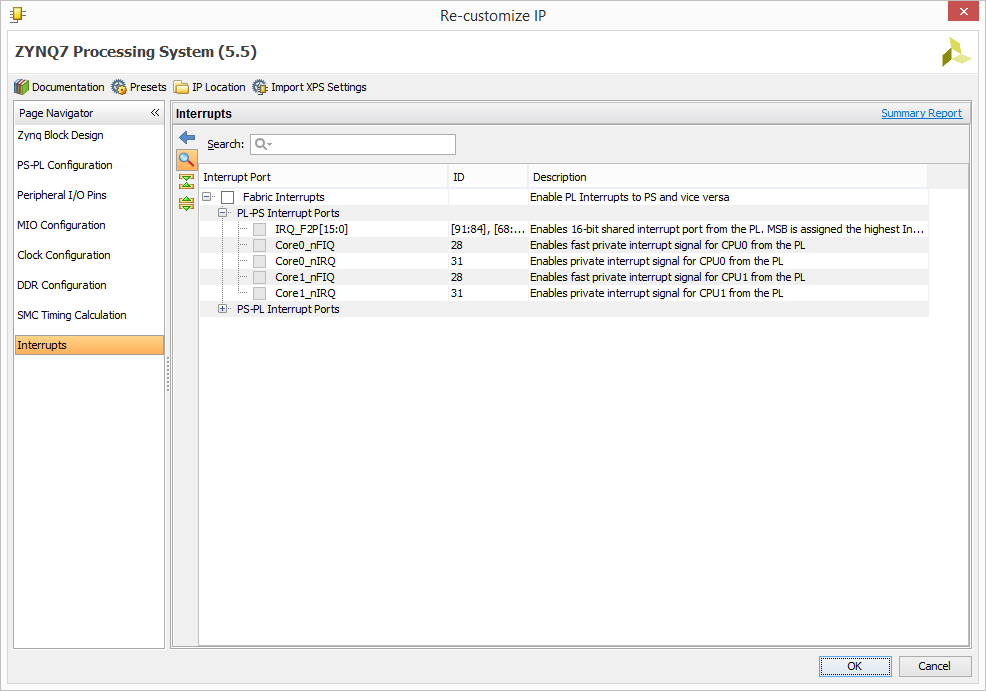
The Interrupts page is another extremely useful one. To use any interrupts with the FPGA, the Fabric Interrupts checkbox must be checked. Many AXI IP cores can be configured to generate an interrupt on some trigger, for instance AXI GPIO cores can be set up to trigger an interrupt whenever an input changes. Checking the IRQ_F2P box in the PL-PS Interrupt Ports drop-down creates a new input port on the Zynq block which can be connected to up to sixteen individual interrupt pins via a Concat (concatenation) IP core. To use interrupts, the 'xscugic' driver for the generic interrupt controller found in the Zynq hardware must be used.
Additionally, interrupts generated by hardware peripherals connected using the Peripheral I/O Pins or MIO Configuration pages can be provided to the FPGA using the fields in the PS-PL Interrupt Ports drop-down.
4.6
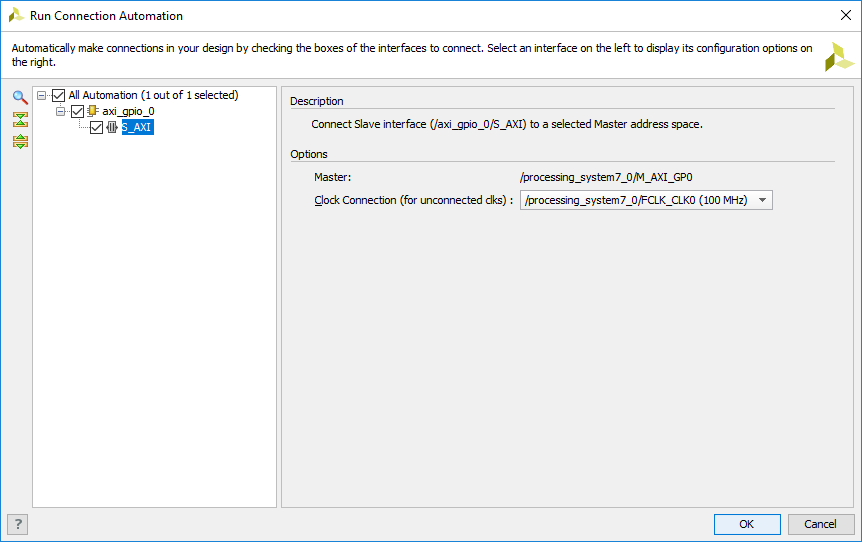
In order to connect the GPIO peripheral to the Zynq block, click Run Connection Automation in the green bar at the top of the block design diagram pane.
In the Run Connection Automation dialog's list pane, make sure that the S_AXI entry is checked and selected.
In the options pane to the right of the dialog, the clock source to run the AXI bus connecting the GPIO IP to the Zynq block can be selected. Select /processing_system7_0/FCLK_CLK0 from the drop-down list.
Click OK to continue.


- Microblaze
-
4.3
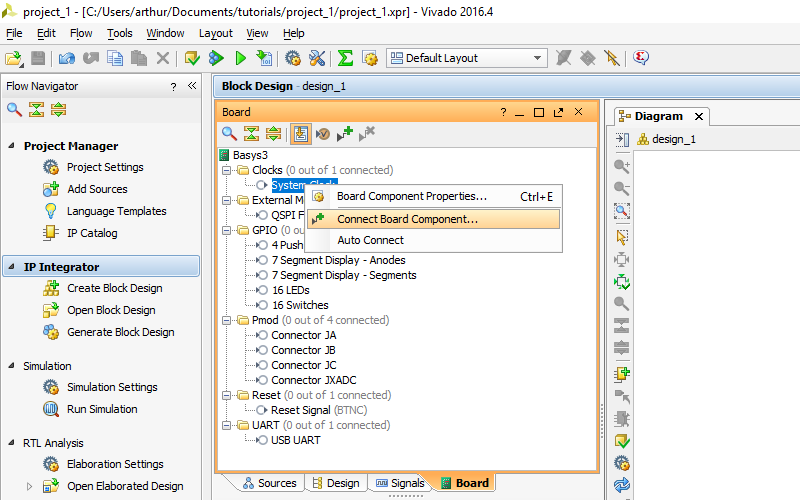
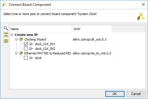
In the Board tab, right click on System Clock and select Connect Board Component.
4.4
In the Connect Board Component dialog make sure that the clock_CLK_IN1 checkbox under Create New IP → Clocking Wizard is checked.
Click OK to continue.
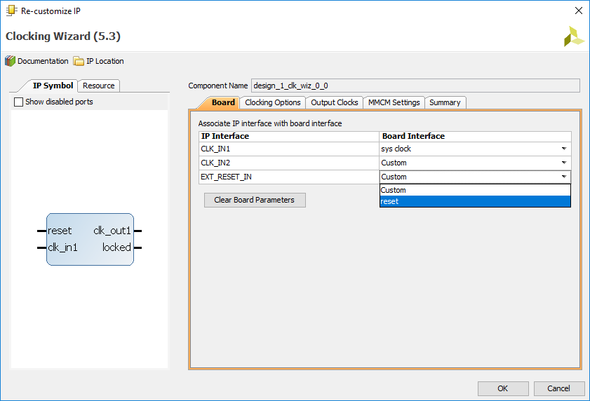
4.5
Double click on the newly created clocking wizard block or select it and click the Customize IP button (
 ).
).
In the Board tab, make sure that sys clock is selected in the CLK_IN1 dropdown, then choose reset from the EXT_RESET_IN drop-down.
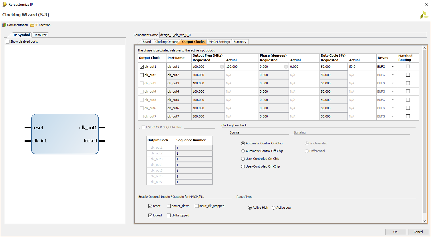
4.6
Select the Output Clocks tab. On this page there are several different options for how to configure the clocking wizard. For the purposes of this guide, the reset type needs to be configured, and a single 100MHz clock needs to be generated.
Make sure that the clk_out1 box is checked and that it's Requested Frequency is 100.000 (MHz).
Depending on how the specific board's reset button works, select Active Low or Active High for the Reset Polarity. The Basys 3 and Cmod A7 are the only boards that use an active high reset polarity at the time of writing.
Click Finish to save changes and continue.
4.7
In the Board tab, right click on the USB UART and select Connect Board Component.
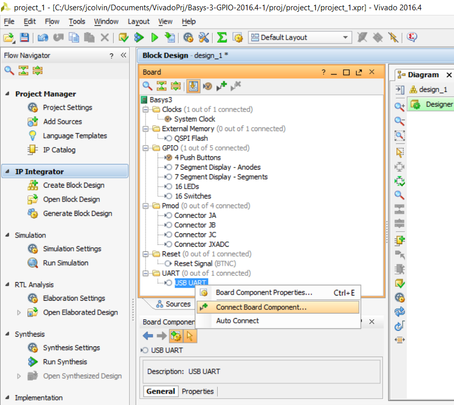
4.8
In the Connect Board Component dialog, make sure to select the AXI Uartlite variant of the IP.
Click OK to continue.

4.9
Click Run Connection Automation in the green bar at the top of the block design diagram pane.
Make sure that the reset entry the list on the left-hand side of the Run Connection Automation dialog is checked and selected. With this box checked, Vivado will automatically connect the reset component selected in the Board pane of the Clocking Wizard Configuration dialog to the clocking wizard, as specified in the Board tab of the Clocking Wizard configuration dialog.
Click OK to continue.

4.10
Click the Add IP button (
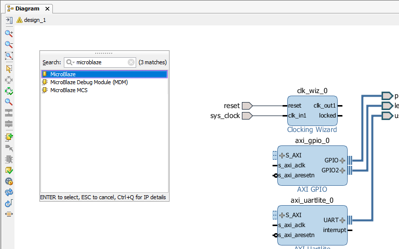
) and search for 'MicroBlaze'. Select MicroBlaze from the list of results and press Enter on the keyboard to continue.
4.11
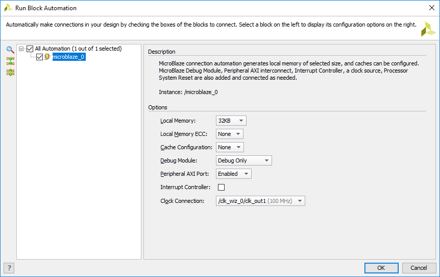
Click Run Block Automation in the green bar at the top of the screen. This will launch a dialog that allows initial configuration of the MicroBlaze and several different IP cores that are key to the function of the design.
In the Run Block Automation dialog, make sure that MicroBlaze_0 under All Automation in the panel to the left is selected and checked.
There are a number of different options available. For the purposes of this guide, set these options to the value found in parentheses below.
- Local Memory (32KB): This option allows the selection of the amount of memory available to the processor. The program to be run on the board must be able to fit in this memory, and this memory must fit within the block RAM available on the board.
- Local Memory ECC (None): This option enables or disables Error Correction in the local memory.
- Cache Configuration (None): This option allows the selection of the size of the Cache. If required, this can be used to speed up memory access.
- Debug Module (Debug Only): This option lets the user select the extent of hardware debug features to be used.
- Peripheral AXI Port (Enabled): This option enables or disables an AXI master port on the MicroBlaze block, which is used to connect the processor to many different Xilinx provided peripheral IP cores.
- Interrupt Controller (Unchecked): This option lets the user select whether or not to automatically generate an interrupt controller, which can be used to trigger the processor to process timing critical functions.
- Clock Connection (/clk_wiz_0/clk_out1): This option allows the user to select which clock source should be used to clock the processor. This can either be a clock that already exists in the design, or block automation can automatically generate a new one.
Click OK to continue.
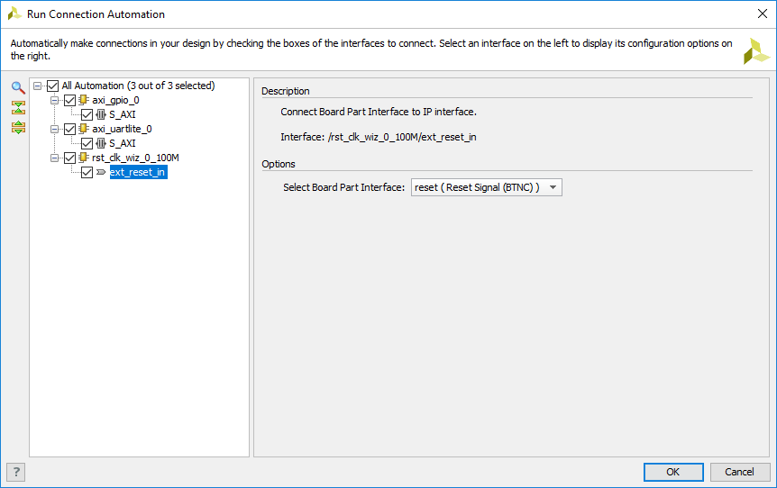
4.12
In order to connect the Uartlite and GPIO peripherals to the MicroBlaze block, click Run Connection Automation. Similarly to the Run Block Automation dialog, the pane to the left of the dialog contains a list of things that can be automated. In this case, the AXI connections for axi_gpio_0 and axi_uartlite_0, as well as the external reset port of the MicroBlaze's reset clocking wizard, are available.
Check the box next to All Automation to make sure that all of three connections will be made.
The clock source for the AXI connection can be changed by selecting the S_AXI entry in the list, and changing the value in the Clock Connection option. Make sure that this option is set to Auto or /clk_wiz_0/clk_out1 for each of the two AXI connections.
The reset source for the MicroBlaze's reset clocking wizard can be changed by selecting the ext_reset_in entry in the list, and changing the value in the Select Board Part Interface option. Make sure that this option is not set to Custom.
Click OK to continue.


5. Generate the Bitstream
5.1
Click the Validate Design button ( ) to have Vivado confirm that everything looks good.
Click OK to continue.

5.2
The last thing that needs to be done before generating a bitstream is to create a top module file. This file will take the block design and interpret it into a hardware design language so that the synthesis and implementation tools can work properly. Right click on the block design in the Sources tab in the pane to the left of the Block Design pane - this pane likely has the Board tab currently selected.
In the right-click menu, select Create HDL Wrapper. In the confirmation dialog that pops up, make sure that Let Vivado manage wrapper and auto-update is selected in the options list. If manual changes need to be made to the wrapper file, the other option here can be selected, but it is not recommended except for advanced users. Click OK to have Vivado finish making the wrapper file.

5.3
With a validated design and a top module, a bitstream can now be generated. The Getting Started with Vivado guide explains this process in a little more detail, but for now, click the Generate Bitstream button in the Flow Navigator.

5.4
The Launch Runs dialog that pops up has several options to choose between. Select Launch runs on local host to actually generate the bitstream now. The other option is to Generate scripts only, which will not generate a bitstream, but rather the scripts required to generate the bitstream on a different machine. The Number of jobs field allows the user to change how much of the resources of the computer Vivado is running on will be used. This process can take some time for complex designs, so it is recommended to devote as much of the resources as possible (typically by selecting '8').
Click OK to continue.

5.5
In the next dialog, No Implementation Results Available, Vivado will ask whether to run Synthesis and Implementation. These steps are required to generate a bitstream, so click Yes.

5.6
Once the bitstream is generated, which may take a little while, Vivado will ask what to do next. None of the available options are required for this guide, so click Cancel.

6. Launch Vivado SDK
Before Vivado SDK can be launched, it needs to be provided with a hardware handoff file, containing the bitstream and various other information about the peripherals installed in the design.
6.1
In the File drop-down, select Export then Export Hardware. This function collects all of the files that SDK needs to program the FPGA and control the hardware instantiated in the design and puts them all into one place.

6.2
Make sure that the Include Bitstream box is checked, so that the FPGA can be programmed from Vivado SDK. The Export Location is <Local To Project> by default. This means that Vivado will create a new directory in the project directory called '<project name>.sdk' where the hardware handoff file - named '<HDL wrapper name>.hdf' - can be found. If a different location is chosen for the hardware handoff file, make sure to remember where it is.
Important
Do NOT use spaces in the export location path. This will cause problems with Vivado. Instead use an underscore, a dash, or CamelCase.
Click OK to continue.

6.3
Just below Export in the File drop-down, select Launch SDK.

6.4
The dialog that pops up will tell Vivado where to find the exported files, as well as where to create the SDK workspace. Make sure to set Exported Location to the location chosen earlier. The Workspace field is <Local To Project> by default. This means that Vivado will use a directory in the project directory called '<project name>.sdk' to store the sources and projects created in Vivado SDK. If this directory does not exist, it will be created. This location can be changed if somewhere else is desired, but it is recommended to leave it as is.
Important
Do NOT use spaces in the workspace path. This will cause problems with Vivado. Instead use an underscore, a dash, or CamelCase.
Click OK to continue.

7. Create a New C Project
7.1
Vivado SDK will now launch, and will import the hardware definition, creating a workspace containing only a hw_platform project. This project contains the files exported from Vivado. There are only a few relevant panes to this guide.
- The Project Explorer, found to the left hand side of the window, displays all projects imported into the workspace, each of which can be expanded to view the sources, scripts, and other files that they contain.
- The File View, directly in the center of the window, displays currently opened files. Upon launch of SDK, an overview of the hardware platform exported from Vivado is displayed. Note the AXI GPIO cell contained in the Address Map, and the corresponding entry in the list of IP blocks.

7.2
In order to create a project to store C source code, click File in the top toolbar, followed by New → Application Project.

7.3
In the New Project dialog, give the project a name, and make sure that C is selected as the Language in the Target Software box.
Important
Do NOT use spaces in the project name. This will cause problems with Vivado. Instead use an underscore, a dash, or CamelCase.
Click Next to continue.

7.4
From the list of Available Templates, select Empty Application, then click Finish.

7.5
Expand the newly created project - not its board support package - then expand the 'src' folder. Right-click on the 'src' folder and select New → Source File from the menu.

7.6
Name the new source file main.c, then click Finish.

7.7
The new main file will now open in the file view pane. Copy-Paste the code to the right into this file, then hit Ctrl-S to save the file and build the project.
//AXI GPIO driver
#include "xgpio.h"

//send data over UART
#include "xil_printf.h"

//information about AXI peripherals
#include "xparameters.h"

int main()
{
	XGpio gpio;
	u32 btn, led;

	XGpio_Initialize(&gpio, 0);

	XGpio_SetDataDirection(&gpio, 2, 0x00000000); // set LED GPIO channel tristates to All Output
	XGpio_SetDataDirection(&gpio, 1, 0xFFFFFFFF); // set BTN GPIO channel tristates to All Input

	while (1)
	{
		btn = XGpio_DiscreteRead(&gpio, 1);

		if (btn != 0) // turn all LEDs on when any button is pressed
			led = 0xFFFFFFFF;
		else
			led = 0x00000000;

		XGpio_DiscreteWrite(&gpio, 2, led);

		xil_printf("\rbutton state: %08x", btn);
	}
}
8. Program and Run the Design
The next step is to program the bit file onto the FPGA and run the C source on the processor.
8.1
From the top toolbar, select Xilinx Tools, then Program FPGA.

8.2
Leave all of the settings in the Program FPGA dialog as they are, then click Program. This only programs the FPGA, not the processor, so that is next.

8.3
Right click on the application project in the Project Explorer, then select Run As → Launch on Hardware (System Debugger).

9. Receiving Messages over UART
9.1
In order to receive UART messages, which are sent by the 'xil_printf' statements in the project's C source code, it is recommended to use a serial console application like Tera Term. The appropriate port to connect to can be determined by reviewing the Device Manager in Windows. Serial Port settings are determined by the configuration of the Zynq block or the AXI Uartlite block's customization settings.
Typically these settings will be 8 Data Bits, No Parity Bit, 1 Stop Bit, and a baud rate of 115200 for Zynq and 9600 for MicroBlaze by default.

Congratulations!
The project will now be running on the board. Press the buttons to see the LEDs flip on and off. Use Tera Term to view the button data in hexadecimal.
Next Steps
Examples of more complicated IPI designs - including examples of the use of DDR memory in MicroBlaze designs - are linked from the target board's resource center, which can be found in this list.