CoolRunner-II Reference Manual
The CoolRunner-II is retired and no longer for sale in our store.
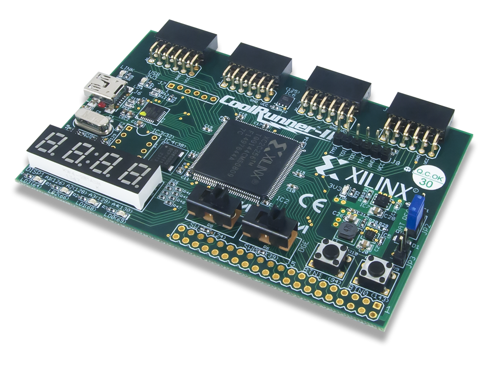
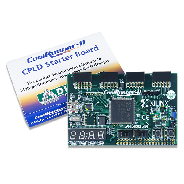
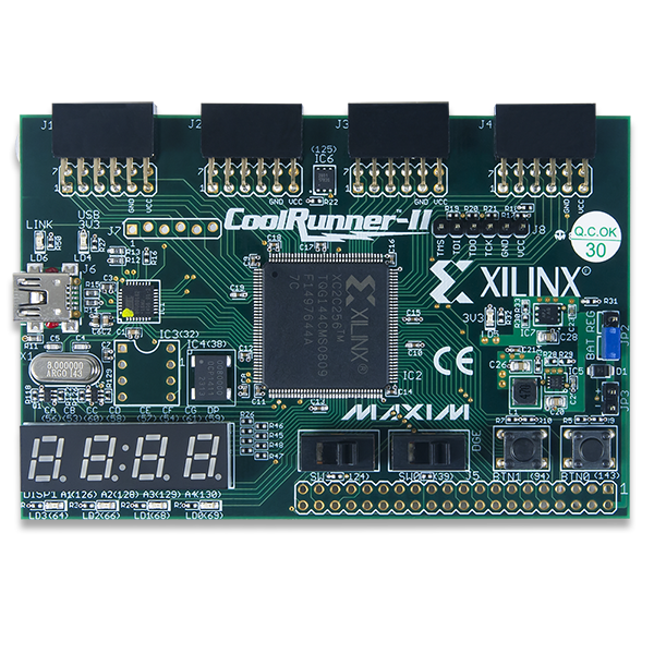
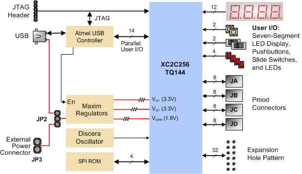
The CoolRunner-II Starter Board is a complete USB-powered circuit development platform for Xilinx's CoolRunner-II CPLD. The board includes highly-efficient power supplies, a programmable oscillator, several I/O devices, and a USB2 port for board power and CPLD programming. The board also includes five expansion connectors that make 64 CPLD signals available to external circuits.

Download This Reference Manual
Features
- a 256-macrocell CoolRunner-II CPLD in a TQ-144 package
- an on-board USB2 port for board power, JTAG programming, and data transfers
- an 8MHz fixed-frequency oscillator and a socket for a crystal oscillator
- expansion connectors for 64 I/O signals (32 on the Pmod ports and 32 on the parallel connector)
- a one-wire DS28E01Q EEPROM
A large collection of board-support IP, reference designs, and add-on peripheral module boards (Pmods) is available at www.digilentinc.com.
Configuration
The CoolRunner-II board's CPLD must be configured (or programmed) by the user before it can perform any functions. Files can be created from schematics or HDL source files using the free ISE WebPack software from Xilinx. Configuration files can be transferred to the CoolRunner-II board using a USB cable and Xilinx's iMPACT software or using an external programming cable (not included). Once configured, the CPLD retains its state indefinitely. When the CoolRunner-II board is powered on, the most recently loaded CPLD configuration is available immediately. A new configuration can be loaded at any time, and as soon as a new configuration is loaded, it defines the CPLD's behavior.
Power Supplies
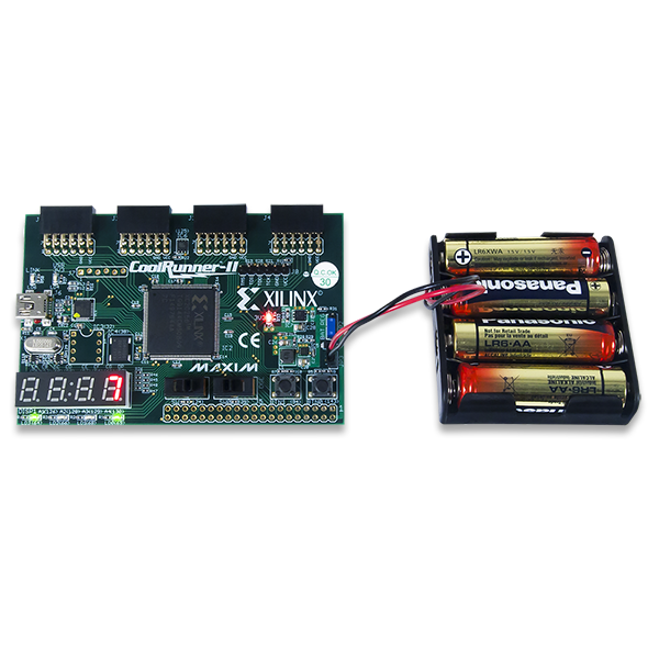
The CoolRunner-II board can be powered from its integral USB port or from an external supply attached at connector JP3. Jumper JP2 selects whether the board uses USB power or external power. External power, from any source, is routed through a Maxim LT3028 regulator to produce the two voltage supplies (3.3V I/O and 1.8V core) required by the CPLD. Whenever board power is applied, the power-on LED glows.
To use an external power source, set jumper JP2 to BAT and apply power to the JP3 pins (see the board's silkscreen for orientation). Any 4.5V to 9V power supply can be used (for example, a transistor battery or a series arrangement of AA cells).
The CoolRunner-II board uses a four-layer PCB, with the inner layers dedicated to VCC and GND. The Maxim regulators, together with good power supply routing and ample bypass capacitors on all IC pins, results in a low-noise power supply.
Clocks
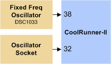
The CoolRunner-II board includes a fixed-frequency oscillator that produces an 8MHz clock signal. This primary oscillator output, labeled PCLK in the schematic, is connected to the GCLK2 pin of the CPLD (at P38) so that it can be routed to the internal clock divider. An unloaded socket for a standard half-size DIP oscillator is also provided at location IC3.
User I/O

The CoolRunner-II board provides two pushbuttons and two slide switches for inputs, and four red LEDs and a four-digit LED display for outputs.
The active-low pushbuttons and slide switches include series resistance for short-circuit protection. The LEDs are active low, and the seven-segment display uses decoupled-transistor active-high common anode signals and active-low cathodes.
Three additional LEDs indicate USB power good (LD4), board power good (LD5), and USB link status (LD6).
Expansion Connectors
The CoolRunner-II board provides four 12-pin peripheral module connectors. Each connector provides two VDD and GND connections and eight unique CPLD signals. Each connector can accommodate a single 12-pin Pmod or two 6-pin Pmods. Digilent makes several 6-pin Pmods that can attach to these connectors, including speaker boards, H-bridge boards, sensor boards, etc. See www.digilentinc.com for more information.
The CoolRunner-II board also provides a 40-pin expansion connector that includes three power-supply signals and 37 individual I/O signals.
Demonstration Design
The design pre-programmed onto the CPLD contains several functions that can be seen when the appropriate peripheral modules are inserted into the relevant ports.
In this sample design, the switch Pmod goes in port J8, the PS/2 Pmod goes in port J7, and the seven-segment display Pmod goes in ports J5 and J6. Of course, the design can be changed to use different ports.
The CPLD implements both a counter as well as a PS/2 keyboard decoder. The display switches between the two based on the value of SW4. SW1, 2, and 3 are not used in the design. BTN0 is the system reset for the design.
When SW4 has the PS/2 decoder selected, the output on the display is the scan code for that letter. Here are some scan codes, the rest can be found on the Internet.
| Keyboard Key | Scan Code |
|---|---|
| F1 | 05 |
| F2 | 05 |
| F3 | 04 |
| F4 | 0C |
| F5 | 03 |
| F6 | 0B |
| F7 | 83 |
| F8 | 0A |
Design Recommendations
- The regulator provides Vccio of 3.3V, so set the Default I/O Standard appropriately.
- Unused I/O should be set to Ground to minimize power.
- Input Termination should be set to Keeper to minimize power consumption on any potentially floating input pins.