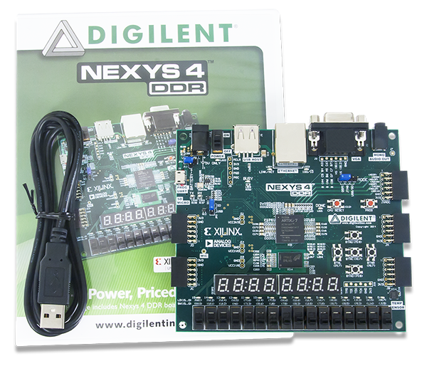
Nexys 4 DDR
- Programmable over JTAG and Quad-SPI Flash
- On-chip analog-to-digital converter
8 flip-flops each)
5 V (2.5 mm coaxial) supply
Important!
This page was created for the Nexys 4 DDR board, revisions A-C. The Nexys 4 DDR has since been rebranded as the Nexys A7, starting in 2018 with revision D. See the Nexys A7 Resource Center for up-to-date materials.
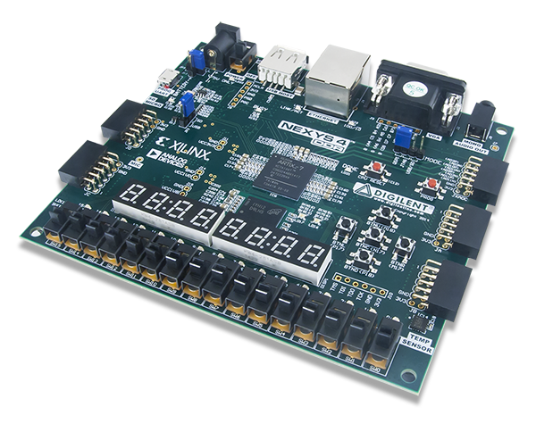
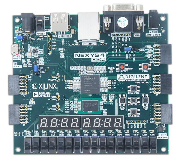
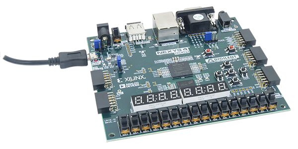
The Nexys 4 DDR board is a complete, ready-to-use digital circuit development platform based on the latest Artix-7™ Field Programmable Gate Array (FPGA) from Xilinx®. With its large, high-capacity FPGA (Xilinx part number XC7A100T-1CSG324C), generous external memories, and collection of USB, Ethernet, and other ports, the Nexys4 DDR can host designs ranging from introductory combinational circuits to powerful embedded processors. Several built-in peripherals, including an accelerometer, temperature sensor, MEMs digital microphone, a speaker amplifier, and several I/O devices allow the Nexys4 DDR to be used for a wide range of designs without needing any other components.
Documentation
Tutorials
- Getting Started with Digilent Pmod IPs
- Getting Started with Vivado
- Getting Started with Vivado IP Integrator and Xilinx SDK
- How To Store Your SDK Project in SPI Flash
- Installing Vivado, Xilinx SDK, and Digilent Board Files
- Nexys 4 DDR - Getting Started with Microblaze Servers
- Nexys 4 DDR Programming Guide
- Programming Digilent FPGA Boards Through Multisim
Example Projects
- Nexys 4 DDR Advanced I/O Demo ( Built-In Self-Test)
- Nexys 4 DDR GPIO Demo
- Nexys 4 DDR Keyboard Demo
- Nexys 4 DDR XADC Demo
Academic Materials
- Example of Coursework using the Nexys 4 DDR – Created by Dr. Victor Nelson for Auburn University's Digital System Design class