SRAM to DDR Component
Download
Description
Note: There is a problem mapping the MIG in ISE. In short, the tools do not see the MIG generated UCF file. This issue can be solved by following the flow found here. The digilent support thread associated with this issue is here.
This component implements a simple asynchronous SRAM interface to DDR2 converter for the Digilent Nexys4-DDR board. It uses the industry-standard SRAM control bus. Read operations are initiated by bringing CEN, OEN and LB/UB low while keeping WEN high. Valid data will be driven out the Data Output port after the specified access time has elapsed. Write operations occur when CEN, WEN and LB/UB are driven low while keeping OEN high.
The LB enable and UB enable signals support byte-wide (8-bit) data writes. During write operations, any disabled bytes will be masked out and not transmitted to the DDR. When both the LB and UB are enabled than word-wide (16-bit) data writes are executed.
This component is particularly useful for those who would like to port a design that targeted an earlier Nexys model and asynchronously accessed the onboard CellRAM. This component shares the same interface, and should allow the previous project to continue to work on the Nexys4-DDR. The only change that must be made is to the read cycle and write cycle wait times. They have increased to 210 and 260 ns, respectively
The converter component instantiates a LogiCORE MIG (Memory Interface Generator) that is configured with the following settings:
| Parameter | Value |
|---|---|
| Controller Type | DDR2 SDRAM |
| Clock Period | 3333 ps (300 MHz) |
| PHY to Controller Clock Ratio | 2:1 |
| Memory Type | Components |
| Memory Part | MT47H64M16HR-25E |
| Data Width | 16 |
| Data Mask | Enabled |
| Ordering | Strict |
| Input Clock Period | 5000 ps (200MHz) |
| Burst Type | Sequential |
| Output Drive Strength | Fullstrength |
| Controller Chip Select Pin | Enable |
| RTT (nominal) – ODT | 50 Ohms |
| Memory Address Mapping Selection | Bank-Row-Column |
| System Clock | No Buffer |
| Reference Clock | Use System Clock |
| System Reset Polarity | Active Low |
| Debug Signals for Memory Controller | Off |
| Internal Vref | Enabled |
| IO Power Reduction | On |
| XADC Instantiation | Enabled¹ |
| Internal Termination Impedance | 50 Ohms |
Table 1. MIG settings
¹If the XADC is used elsewhere in the design, this should be disabled. It is disabled in the Ram2Ddr version of this core
This project contains two different components: Ram2Ddr and Ram2DdrXadx. If your design does not use the XADC core anywhere else, you should use the Ram2DdrXadc component. It automatically instantiates the XADC internally to monitor the chip temperature. If your design does use the XADC core, you should use the Ram2Ddr component. You will then have to connect the device_temp line of the Ram2Ddr component to the XADC component, as described on page 122 in version 1.9 of Xilinx's 7 Series FPGAs Memory Interface Solutions Guide (UG586).
Components can either be inserted into a project as a pre-compiled netlist (.ngc), or as sources by copying the VHDL and MIG project files into your project. Both are included with the download.
Port Descriptions
Figure 1 shows the ram2ddr component block diagram with its ports:
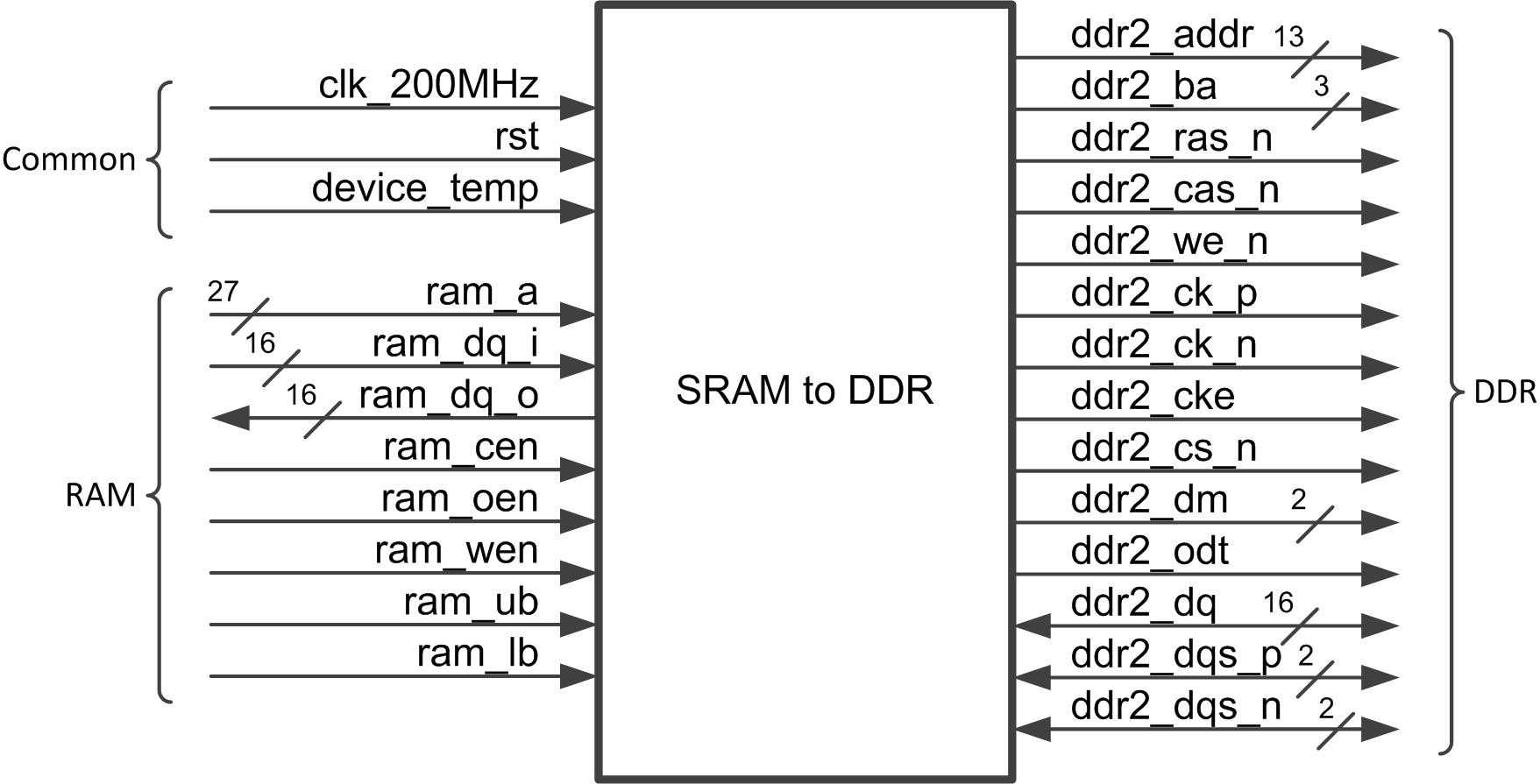 Figure 1. Block Diagram
| Port | Direction | Description |
|---|---|---|
| clk_200MHz | Input | Single-ended, buffered 200 MHz clock input |
| rst | Input | Active-high global reset |
| device_temp | Input | This port is active only in the ram2ddr.ngc file (where the XADC module is not internally instantiated) and shall be tied to GND in the ram2ddrxadc.ngc component. See “Xilinx UG586 7 Series FPGAs Memory Interface Solutions” for more details on driving this port. |
| RAM | ||
| ram_a (26:0) | Input | Input address |
| ram_dq_i (15:0) | Input | Data input |
| ram_dq_o (15:0) | Output | Data output |
| ram_cen | Input | Active-low Chip Enable |
| ram_oen | Input | Active-low Output Enable |
| ram_wen | Input | Active-low Write Enable |
| ram_ub | Input | Active-low Upper Byte select |
| ram_lb | Input | Active-low Lower Byte select |
| DDR | ||
| ddr2_addr (12:0) | Output | Memory Address output |
| ddr2_ba (2:0) | Output | Bank Address |
| ddr2_ras_n | Output | Active-low Row Address Strobe |
| ddr2_cas_n | Output | Active-low Column Address Strobe |
| ddr2_we_n | Output | Active-low Write Enable |
| ddr2_ck_p, ddr2_ck_n | Output | Differential Memory Clock output |
| ddr2_cke | Output | Active-high Memory Clock Enable |
| ddr2_cs_n | Output | Active-low Chip Select |
| ddr2_dm (1:0) | Output | Output Data Mask |
| ddr2_odt | Output | On-Die Termination |
| ddr2_dq (15:0) | Bidirectional | Data input/output bus |
| ddr2_dqs_p (1:0), ddr2_dqs_n (1:0) | Bidirectional | |
Table 2. Port Descriptions
Bus Timing
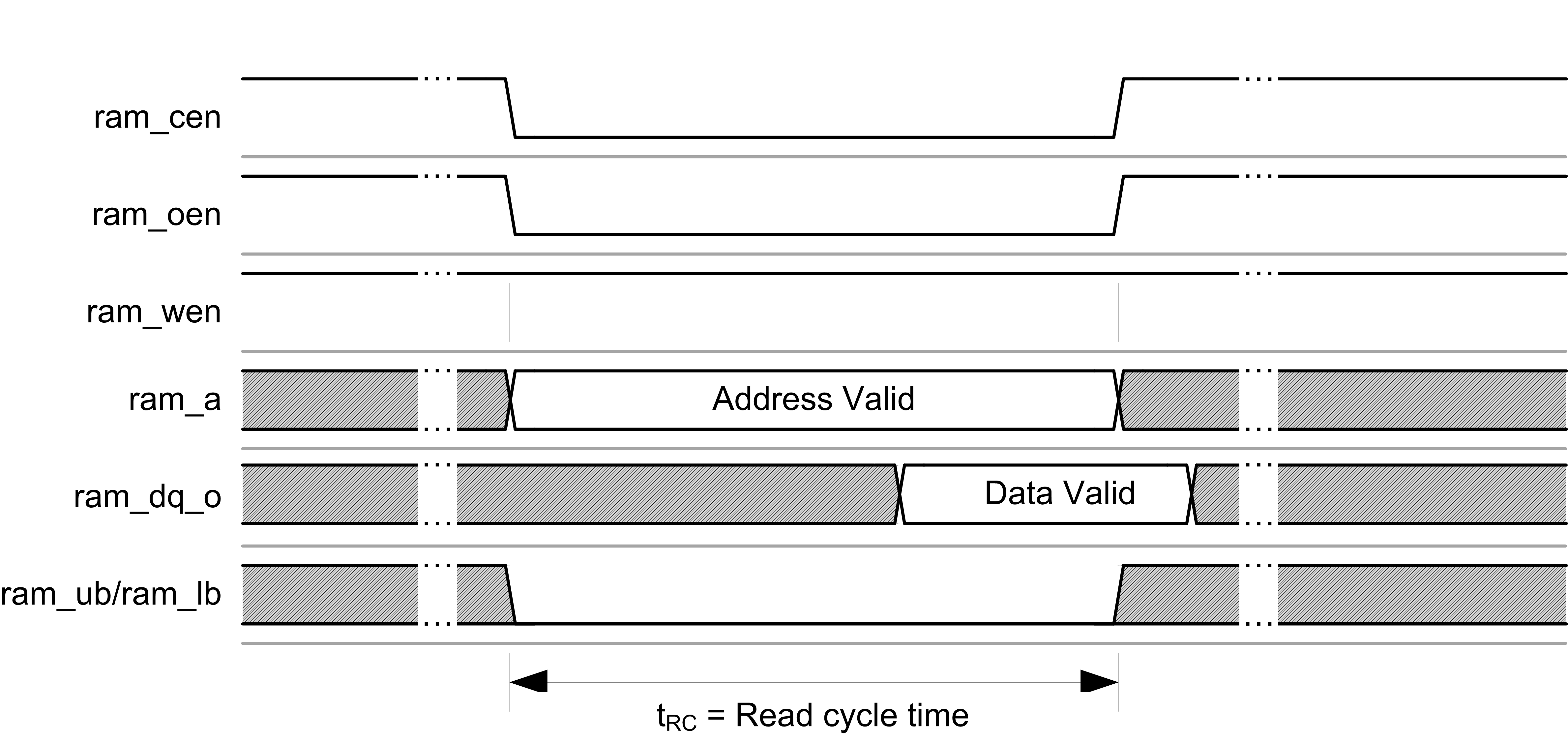 Figure 2. Read Operation
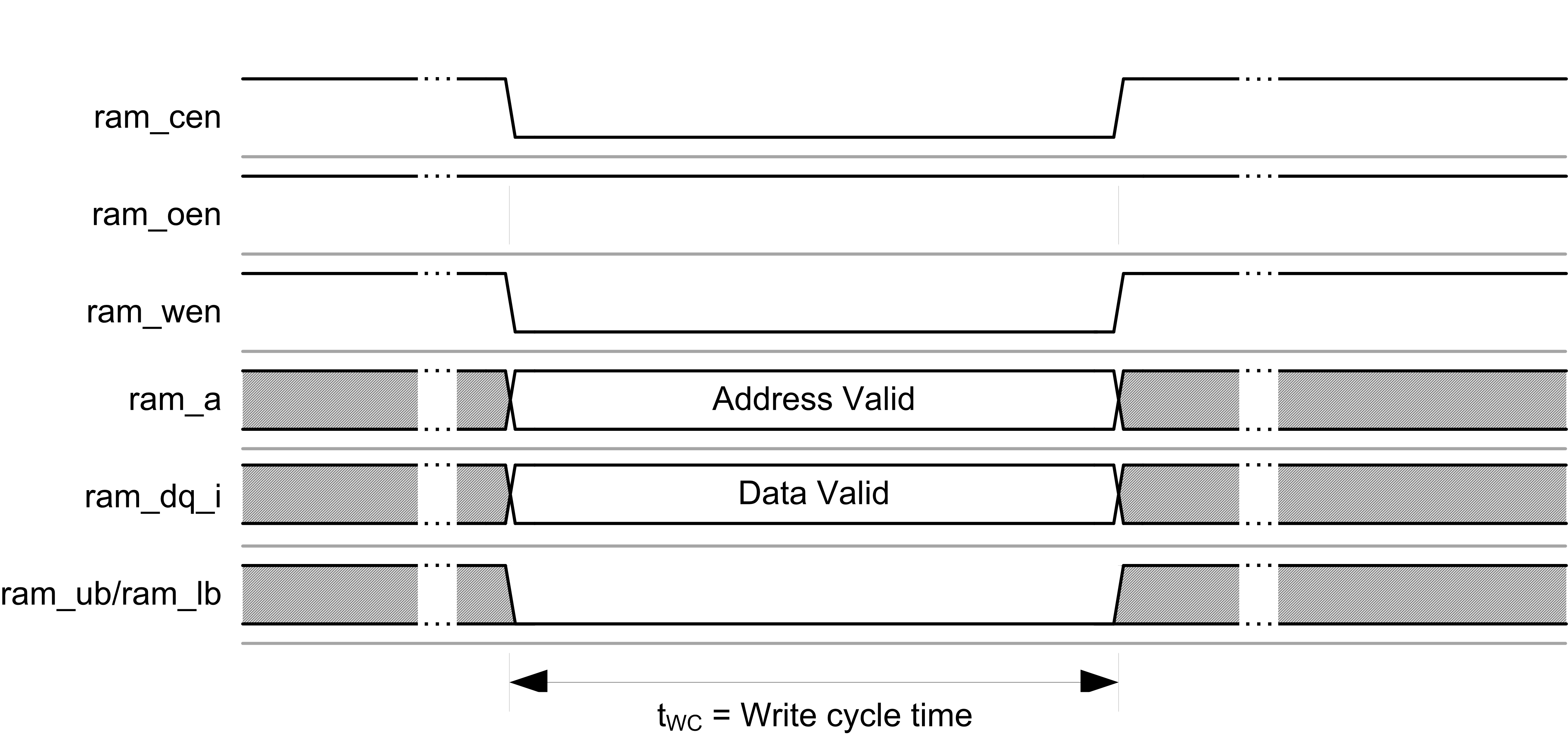 Figure 3. Write Operation
| Parameter | Symbol | Min | Max | Unit |
|---|---|---|---|---|
| Read cycle time | tRC | 210 | - | ns |
| Write cycle time | tWC | 260 | - | ns |
Usage with Other Boards
In order to use this reference component with boards other than the Digilent Nexys4-DDR, the following should be modified:
- Memory Interface Generator must be rerun and the following must be changed:
- Controller Type and/or Memory Part (depending on the memory)
- Controller Chip Select Pin (depending on the board)
- RTT (nominal) – On Die Termination (depending on the board)
- Internal Vref (depending on the board)
- Internal Termination Impedance (depending on the board).
- Pin constraints must be changed to match how the DDR2 is connected on the new board
- Update the instantiation of the MIG component according to the new settings