Arty - Getting Started with Microblaze
Important!
This guide is obsolete, the updated guide can be found here.

Overview
This guide will provide a step by step walk-through of creating a Microblaze based hardware design using the Vivado IP Integrator for the Arty FPGA board.
At the end of this tutorial you will have:
- Created a Microblaze based hardware ( HW ) design in Xilinx Vivado
- Created .C Project in Xilinx Vivado SDK ( Software Development Kit) to display Hello World through hardware design.
- Displayed the final output on both the SDK console and Tera Term
Introduction to MicroBlaze
Microblaze is a soft IP core from Xilinx that will implement a microprocessor entirely within the Xilinx FPGA general purpose memory and logic fabric. For this tutorial, we are going to add a Microblaze IP block using the Vivado IP Integrator tool.
In addition to the Microblaze IP block, we would also like to make use of the DDR3 SDRAM component on the Arty. Therefore a MIG ( Memory Interface Generator ) IP block will be added to our design.
Finally, a UART ( universal asynchronous receiver/transmitter ) IP block will be added to communicate between the host PC and the soft processor core running on the Arty.
General MicroBlaze Design Flow
I. Vivado
- Open Vivado and select Arty board
- Create an new Vivado Project
- Create empty block design workspace inside the new project
- Add required IP blocks using the IP integrator tool and build Hardware Design
- Validate and save block design
- Create HDL system wrapper
- Run design Synthesis and Implementation
- Generate Bit File
- Export Hardware Design including the generated bit stream file to SDK tool
- Launch SDK
Now the Hardware design is exported to the SDK tool. The Vivado to SDK hand-off is done internally through Vivado. We will use SDK to create a Software application that will use the customized board interface data and FPGA hardware configuration by importing the hardware design information from Vivado.
II. SDK
- Create new application project and select default Hello World template
- Program FPGA
- Run configuration by selecting the correct UART COM Port and Baud Rate
Prerequisites
Skills
- Familiarity with Vivado
- Block Design Experience
Hardware
- Digilent Arty FPGA Board
- Micro USB Cable
- Used for UART communication, JTAG programming, and Power
Software
- Xilinx Vivado 2015.4 with the SDK package.
- Newer versions of Vivado may also work
- Digilent Board Support Files
- Follow the wiki guide on how to install Board Support Files for Vivado 2015.X
Tutorial
1. Creating a New Project
1.1) Open up Vivado and click Create New Project to open Vivado's New Project wizard.

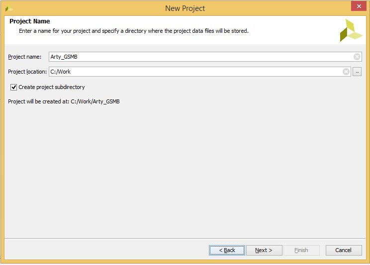
1.2) A new window will open up, click Next and you'll see the screen below. Name your project (no spaces!) and choose your project saving directory before clicking Next. Underscores are a good substitute for empty spaces.
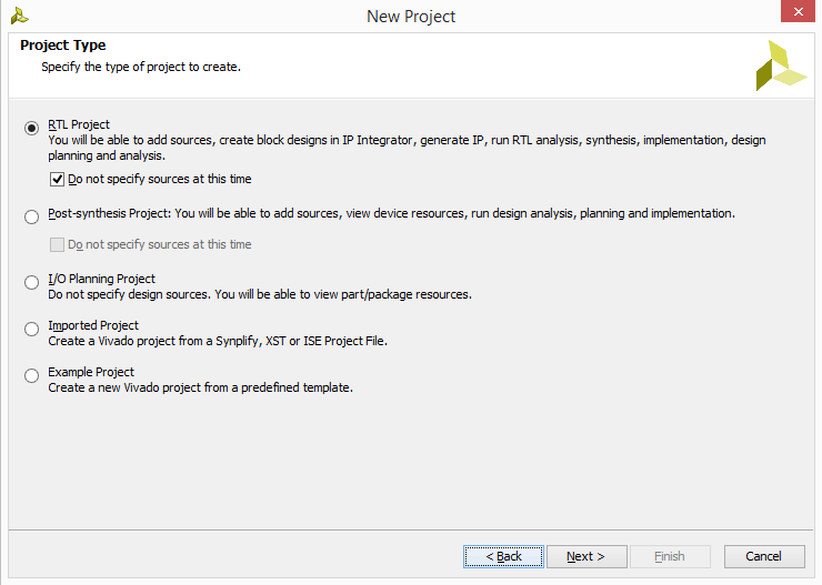
1.3) We will be building this project from the ground up and adding our own sources so we will want to create an RTL project. Select RTL Project and make sure the Do not specify sources at this time box is checked. Click Next.
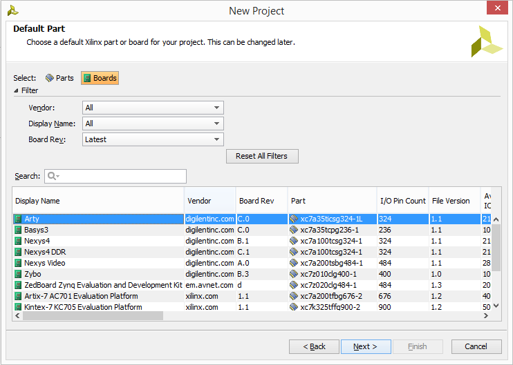
1.4) If you have followed the Board Support File Wiki guide then select Boards. The filter options can be used to quickly find the Arty board, by selecting “digilentinc.com” for Vendor, and “Arty” for Display Name. Arty should be displayed in the selection list. Selecting a different board name will cause errors later. Click Next.
1.5) A summary of the new project design sources and target device is displayed. Click Finish.

At this point you have successfully created a project that will properly communicate with the Arty.
2. Creating New Block Design
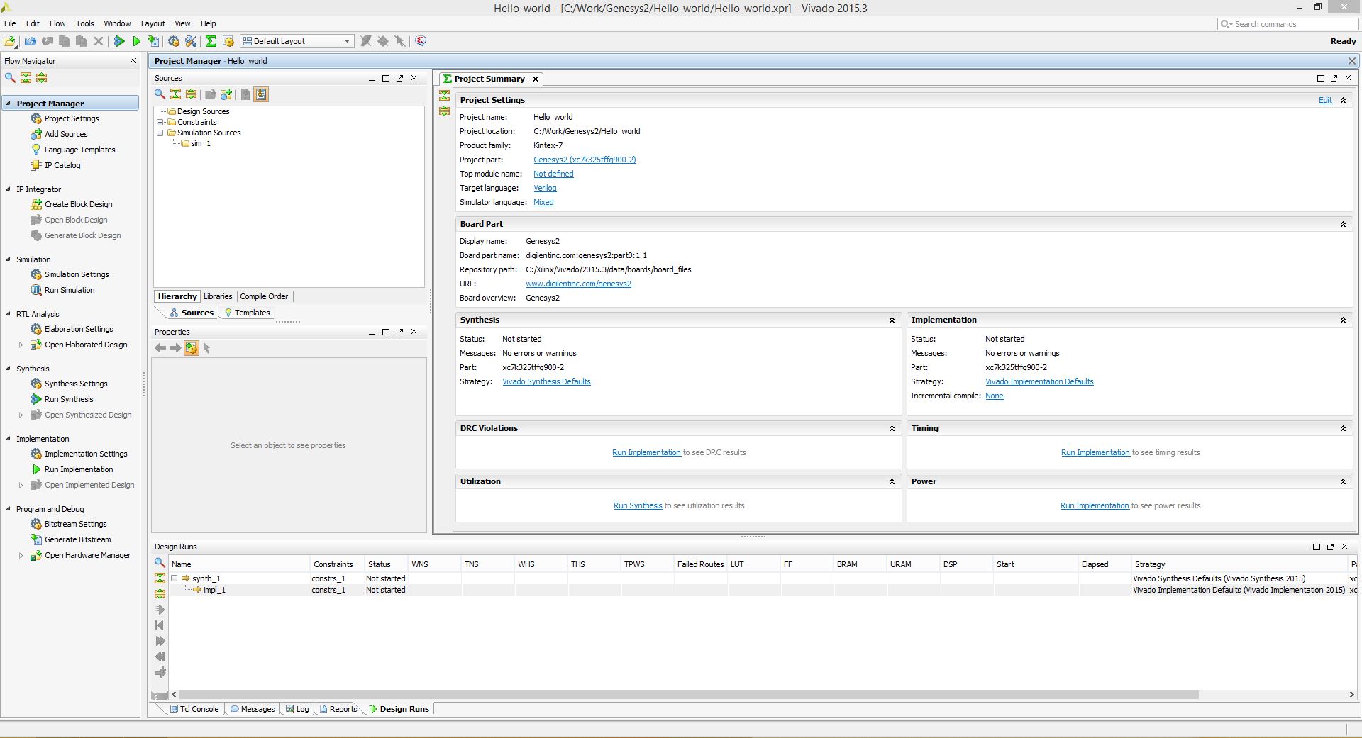
This is the main project window where you can create a IP based block design or add RTL based design sources. The flow navigator panel on the left provides multiple options on how to create a hardware design, perform simulation, run synthesis and implementation and generate a bit file. You can also program the board directly from Vivado with the generated bit file for an RTL project using the Hardware Manager.
For our design, we will use the IP Integrator to create a new block design.
2.1) On the left you should see the Flow Navigator. Select Create Block Design under the IP Integrator. Give a name to your design (without any empty spaces) and click OK.
You have created a new block design.

3. Adding the clock and DDR3 Component
3.1) Click the Board tab (Highlighted in orange below)
This list contains all of the components defined in the board file you installed before. These are already configured to work with several Vivado IPs.
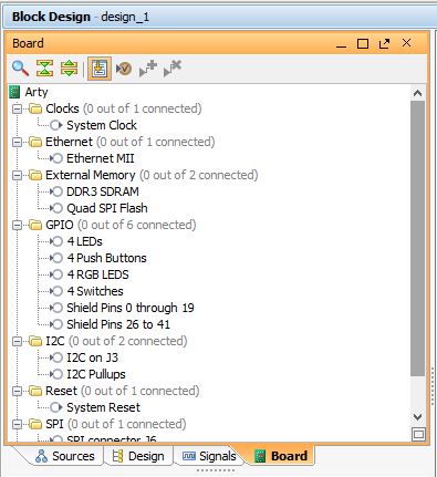
3.2) Click and drag the System Clock component onto the empty block design. Vivado will automatically connect this system clock to a new Clocking Wizard block.
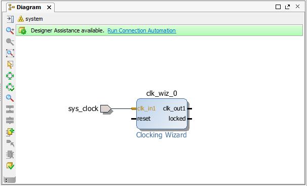
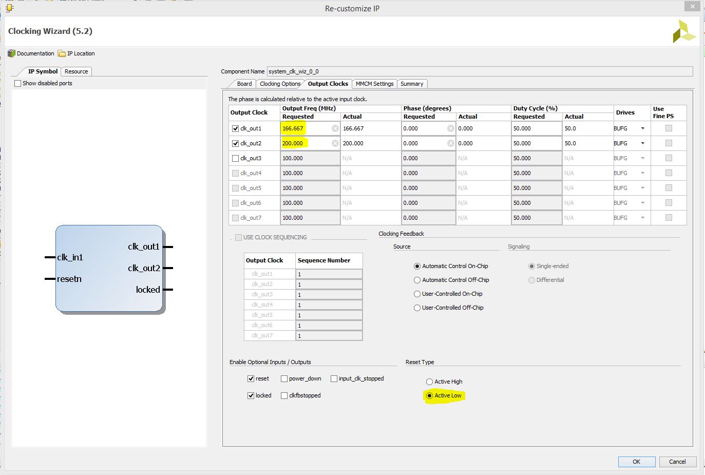
3.3) Double click the Clocking Wizard block to customize it. Click on the Output Clocks tab and change clk_out1 to “166.667” MHz. Enable clk_out2 and set it to “200.0” MHz. Set the Reset Type to Active Low
Click OK to close this window.
3.4) Click and drag the DDR3 SDRAM component onto the empty block design. Vivado will automatically connect the DDR3 SDRAM and some dummy clock ports to the MIG IP.
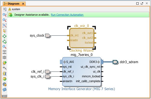
3.5) Delete the clk_ref_i and sys_clk_i ports by clicking them and pressing the Delete key, or by right clicking them and selecting Delete.
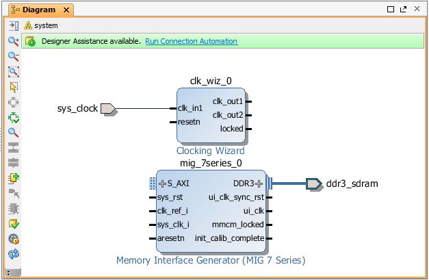
3.6) Connect clk_out1 to sys_clk_i on the MIG block. Connect clk_out2 to clk_ref_i.
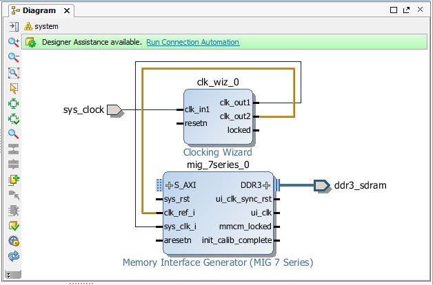
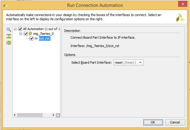
3.7) Click Run Connection Automation in the green banner above. The default settings are fine, so click OK.
Vivado will connect your system reset to sys_rst on the MIG. Connect this new reset port to the resetn input on the Clock Wizard block.
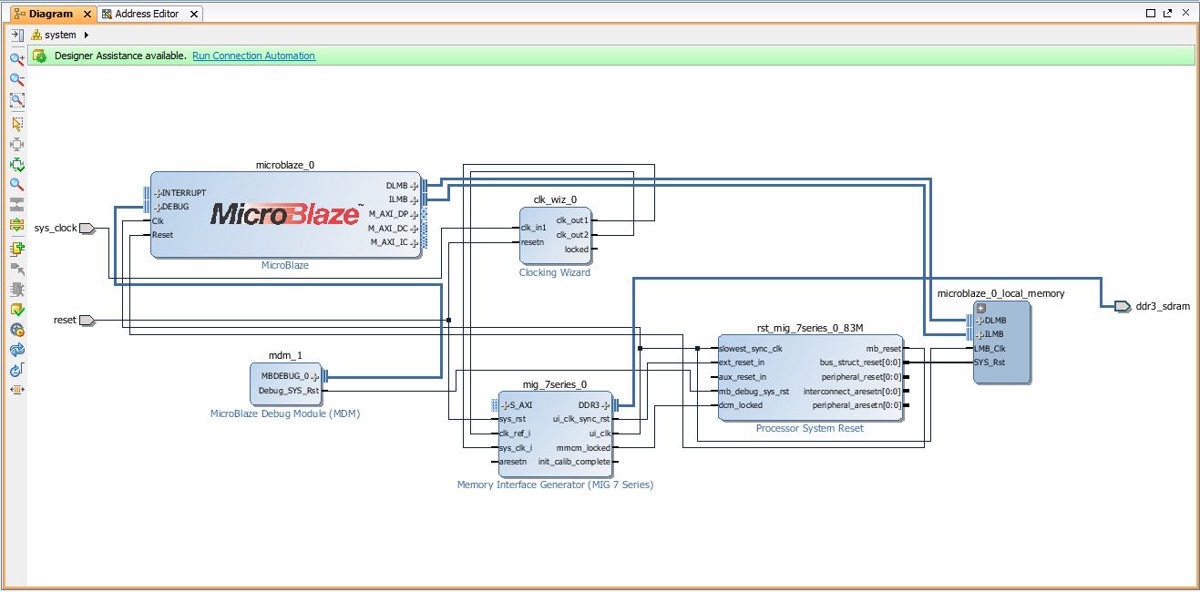
4. Adding the Microblaze Processor & Configuration
4.1) Click theAdd IP button and search for Microblaze.
Double click Microblaze to add it to your block design.


4.2) Click Run Block Automation to open the Block automation for the Microblaze processor.
Here you can choose how much memory to give your Microblaze processor. Configure the options to match the picture below, then click OK. Make sure that you set the Clock Connection to /mig_7series_0/ui_clk.
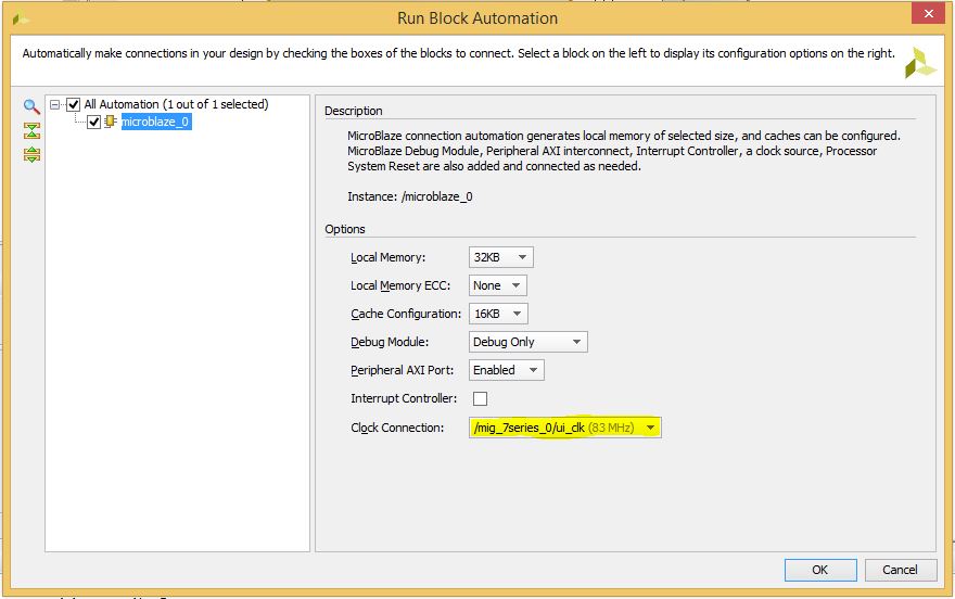
4.3) Running the block automation will auto-generate a set of additional IP blocks which will be added to our hardware design automatically based on the options selected in the previous step. Do Not click on Run Connection Automation yet.
5. Adding Peripheral Components
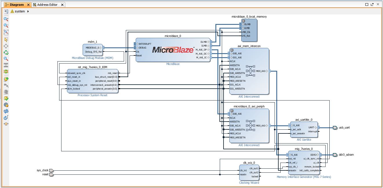
5.1) Go into the Boards tab again and find the USB UART component. Click and drag this onto the block design to add the Uartlite block to your design.

5.2) Click Run Connection Automation in the green banner. Check the All Automation checkbox and click OK.
This will create one AXI Interconnect for the DDR Memory and another for peripheral components.
Click theRegenerate Layout button to rearrange your block design.

6. Validating Design and making an HDL Wrapper
6.1) SelectValidate Design. This will check for design and connection errors.
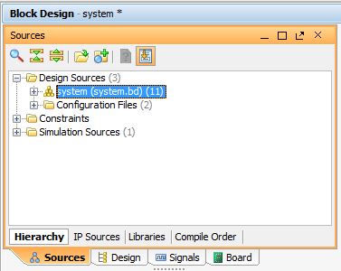
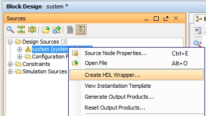
6.2) After the design validation step we will proceed with creating a HDL System Wrapper. Click on the Sources tab and find your block design.
Right click on your block design and click Create HDL Wrapper. Make sure Let Vivado manage wrapper and auto-update is selected and click OK.
This will create a top module in Verilog and will allow you to generate a bitstream.
7. Generating Bit File
7.1) In the top toolbar in Vivado, clickGenerate Bitstream. This can also be found in the Flow Navigator panel on the left, under Program and Debug.
If you haven't already saved your design, you will get a prompt to save the block design.
7.2) The bit file generation will begin. The tool will run Synthesis and Implementation. After both synthesis and implementation have been successfully completed, the bit file will be created. You will find a status bar of Synthesis and Implementation running on the top right corner of the project window.
This process can take anywhere from 2 to 20 minutes depending on your computer.
7.3) After the bitstream has been generated, a message prompt will pop-up on the screen. You don't have to open the Implemented Design for this demo. Just click Cancel.
8. Exporting Hardware Design to SDK
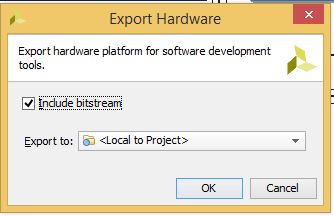
8.1) On the main toolbar, click File and select Export→Export Hardware. Check the box to Include Bitstream and click OK. This will export the hardware design with system wrapper for the Software Development Tool - Vivado SDK.
A new file directory will be created under Hello_World.SDK similar to the Vivado hardware design project name. Two other files, .sysdef and .hdf are also created. This step essentially creates a new SDK Workspace.
8.2) On the main toolbar, click File and then Launch SDK. Leave both of the dropdown menus as their default Local to Project and click OK. This will open Xilinx SDK and import your hardware.

9. Inside Xilinx SDK
9.1) The HW design specification and included IP blocks are displayed in the system.hdf file. Xilinx SDK is independent of Vivado, i.e. from this point, you can create your SW project in C/C++ on top of the exported HW design. If necessary, you can also launch SDK directly from the SDK folder created in the main Vivado Project directory.
From this point, if you need to go back to Vivado and make changes to the HW design, then it is recommended to close the SDK window and make the required HW design edits in Vivado. After this you must follow the sequence of creating a new HDL wrapper, save design and bit file generation. This new bit file and system wrapper must then be exported to SDK.

9.2) Within the Project Explorer tab on the left, you can see your hardware platform.
system is the name of your block design created in Vivado. This hardware platform has all the HW design definitions, IP interfaces that have been added, external output signal information and local memory address information.
10. Creating New Application Project in SDK
10.1) Click theNew dropdown arrow and select Xilinx→Application Project.
Give your project a name that has no empty spaces and click Next.

10.2) Select Hello World from the list of templates and click Finish.

You will see two new folders in the Project Explorer panel.
- Hello_world which contains all the binaries, .C and .H (Header) files
- Hello_world_bsp which is the board support folder
Hello_world is our main working source folder. This also contains an important file shown here which is the “lscript.ld”. This is a Xilinx auto generated linker script file. Double click on this file to open.
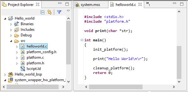
10.3) Back in the Project Explorer, double click and open helloworld.c under the src folder.
This is the main .C file which will print “Hello World” in the console when executed.
11. Programming FPGA with Bit File
11.1) Make sure that the Arty is turned on and connected to the host PC via the USB-JTAG port - this port will serve dual purpose as the USB-UART connection to the Microblaze.
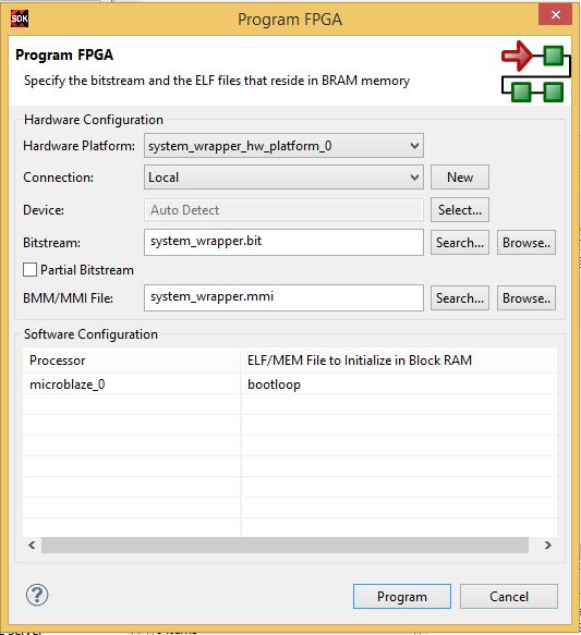
On the top toolbar, click theProgram FPGA button.
11.2) Click Program to program your FPGA with your hardware design.
12. Setting up UART Terminal
12.1) Open up a Serial Terminal application (Tera Term). Connect to the Arty UART port with a baud rate of 9600. This baud rate can be altered in your block design by double clicking the Uartlite block.

13. Program the Microblaze Processor
13.1) Back in SDK, select your Hello_world project and click theRun As… button. Select Launch on Hardware (System Debugger) and click OK.

13.2) Your program will run and you should see “Hello World” pop up inside of your Serial Terminal. Hooray!
