Zmod AWG Reference Manual
Formerly known as Zmod DAC.
The Digilent Zmod AWG, is an open-source hardware SYZYGY™ 1) compatible pod containing a dual-channel DAC and the associated front end. The Zmod AWG is intended to be used with any SYZYGY™ compatible carrier board having the required capabilities.
The analog outputs can be connected to a circuit using SMA cables. Driven by the SYZYGY™ carrier, the Zmod AWG can generate two simultaneous signals (50Ω, ±5V, single-ended, 14-bit, 100MS/s, 40MHz+ bandwidth).
The Zmod AWG was designed to be a piece in a modular, HW and SW open-source ecosystem. Combined with a SYZYGY™ carrier, other SYZYGY™ compatible pods, Zmod AWG can be used for a variety of applications: data acquisition systems, closed loop controllers, etc.
Overview
This document describes the Zmod AWG's circuits, with the intent of providing a better understanding of its electrical functions, operations, and a more detailed description of the hardware’s features and limitations. It is not intended to provide enough information to enable complete duplication of the Zmod AWG, but can help users to design custom configurations for programmable parts in the design.
Features
- Channels: 2
- Channel type: single ended
- Resolution: 14-bit
- Output Range: ±1.25V (Low Range); ±5V (High Range)
- Absolute Resolution: 167μV (Low Range); 665μV (High Range)
- Accuracy - typical ± 0.2% of Range
- Output impedance: 50Ω
- Sample rate (real time): 100MS/s.
- AC amplitude (max): ±5 V.
- Analog bandwidth: 40 MHz @ 3dB, 20 MHz @ 0.5dB, 14 MHz @ 0.1dB
- Slew rate (2V step): 180V/μs
1. Architectural Overview and Block Diagram
Zmod AWG's high-level block diagram is presented in Fig. 2 below. The core of the Zmod AWG is the dual channel, high speed, low power, 14-bit, 125MS/s DAC, AD9717. The carrier board is responsible to configure the internal registers of the DAC circuit, provide the acquisition clock and generate the data.
The Analog Output block is also called the AWG (Arbitrary Waveform Generator), because of similar structure and behavior to such a front end. The signals in this circuitry use “AWG” indexes, to indicate they are related to the AWG block. Signal and equations also use certain naming conventions. Analog voltages are prefixed with a “V” (for voltage), and suffixes and indexes are used in various ways: to specify the location in the signal path (OUT, DAC, etc.); to indicate the related instrument (AWG, etc.); and to indicate the channel (1 or 2). Referring to the block diagram in Fig. 2 below:
- The Arbitrary Outputs/AWG instrument block includes:
- DAC: the digital-to-analog converter for both AWG channels
- AWG ref: reference voltage for the DAC
- I/V: current to bipolar voltage converters
- Out: output stages
- Protection: output stages protection circuitry
- The Power Supplies and Control block generates all internal supply voltages.
- The MCU works as a I2C memory for two different purposes:
- The DNA includes the standard SYZYGY™ pod identification information.
- The Calibration Memory stores all calibration parameters. The Zmod AWG includes no analog calibration circuitry. Instead, a calibration operation is performed at manufacturing (or by the user), and parameters are stored in memory. The application software uses these parameters to correct the generated signals
In the sections that follow, schematics are not shown separately for identical blocks. For example, the AWG I/V schematic is only shown for channel 1 since the schematic for channel 2 is identical. Indexes are omitted where not relevant. As examples, in equation \ref{2} below, $V_{outAWGFS}$ does not contain the channel index (because the equation applies to both channels 1 and 2).
Figure 2. Zmod AWG Block diagram.
2. Arbitrary Waveform Generator
2.1. AWG Reference
As shown in Fig. 3, the reference voltage for the AWG is generated by IC42 (ADR3412ARJZ).
- Initial accuracy: ±0.1% (maximum)
- Maximum temperature coefficient: 8 ppm/°C
- Operating temperature range: −40°C to +125°C
- Output current: +10 mA source/−3 mA sink
- Low quiescent current: 100 μA (maximum)
- Low dropout voltage: 250 mV at 2 mA
- Output noise (0.1 Hz to 10 Hz): <10 μV p-p at 1.2 V (typical)
A divided version is provided to the DAC:
$$V_{REFIO\_AWG}=V_{REF1V2\_AWG} \cdot \frac{R_{27}}{R_{26}+{R_{27}}}=1V\label{1}\tag{1}$$
Figure 3. Reference voltage.
2.2. AWG DAC
The Analog Devices AD9717 dual, low-power 14-bit TxDAC digital-to-analog converter is used to generate the wave. The main features are:
- Power dissipation @ 3.3V, 2 mA output: 86 mW @ 125MS/s, sleep mode: <3 mW @ 3.3V
- Supply voltage: 1.8V to 3.3V
- SFDR to Nyquist: 84 dBc @ 1 MHz output, 75 dBc @ 10 MHz output
- AD9717 NSD @ 1 MHz output, 125MS/s, 2 mA: −151 dBc/Hz
- Differential current outputs: 1 mA to 4 mA
- CMOS inputs with single-port operation
- Output common mode: 0 to 1.2 V
- Small footprint, 40-lead LFCSP RoHS-compliant package
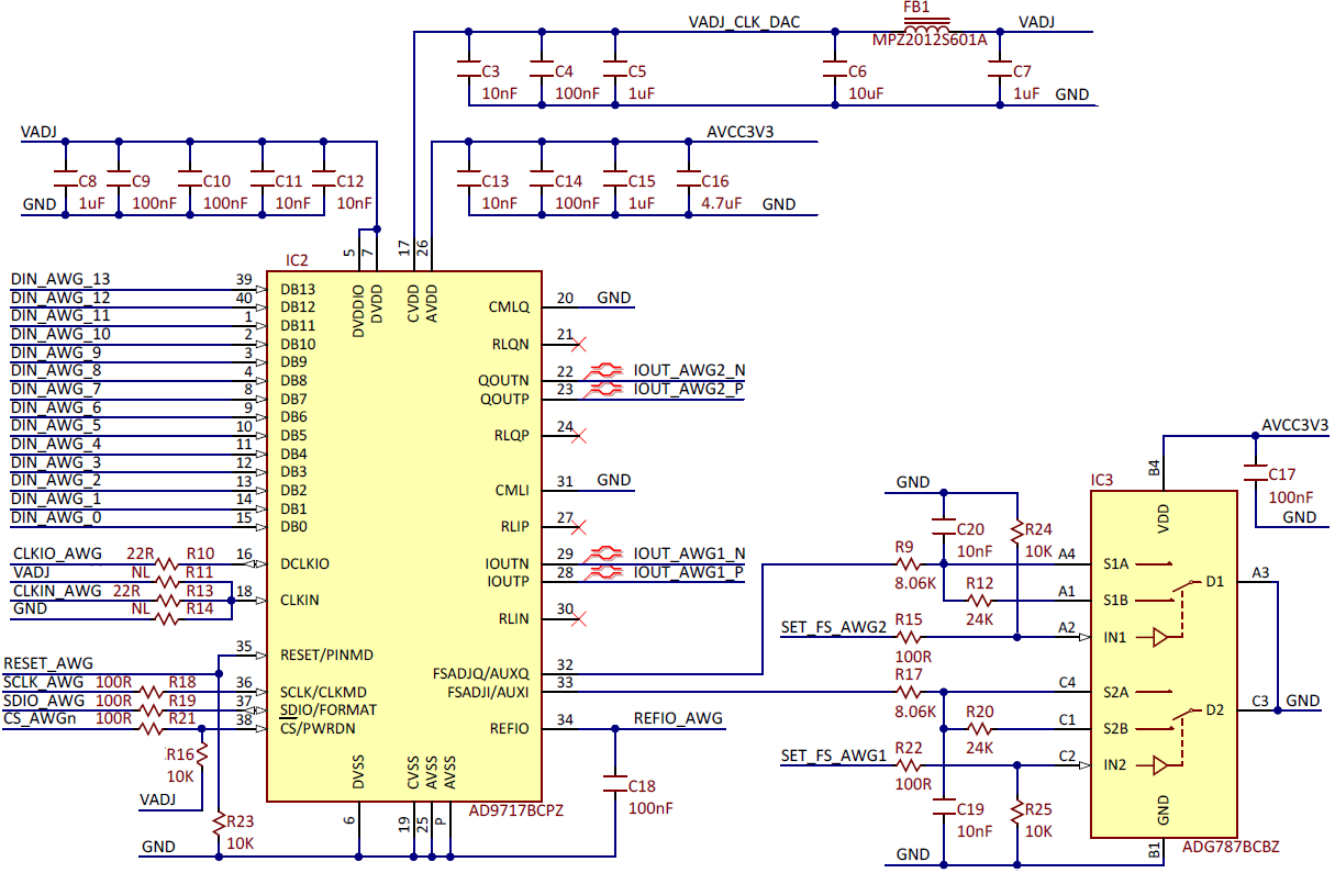
The parallel Data Bus, the single ended 100 MHz clock and the SPI configuration bus are driven by the SYZYGY™ carrier board FPGA. External VREFIO_AWG reference voltage is used. The Full Scale is set via the FSADJx pins. The ADG787 2.5Ω CMOS Low Power Dual 2:1 MUX/DEMUX is used to connect ${{\text{R}}_{set}}$ of either 8kΩ (for high gain) or 32kΩ (for low gain) from FSADJx pin to GND.
The Full Scale DAC output current is:
$$I_{outAWGFS}=32 \cdot \frac{V_{REFIO\_AWG}}{R_{set}}\label{2}\tag{2}$$
For high-gain (High Range):
$$I_{outAWGFS\_HG}=32 \cdot \frac{1V}{8.06k \Omega}=3.97mA\label{3}\tag{3}$$
For low-gain (Low Range):
$$I_{outAWGFS\_HG}=32 \cdot \frac{1V}{32k \Omega}=1mA\label{4}\tag{4}$$
The ADG787 features:
- −3 dB bandwidth, 150 MHz
- Single-supply 1.8V to 5.5V operation
- Low on resistance: 2.5 Ω typical
2.3. AWG I/V
2.4. AWG Out
The AWG Out stage is the output stage of the AWG. It provides the 50ohm output impedance signal and protection to accidental shorts.
The output voltage range depends on High-gain versus Low-gain selection:
$$ - HighRange= - 5.32V < - 5V < V_{AWG\;REL\;HG} < 5V < 5.32V = HighRange $$ $$ -LowRange = - 1.33V < 1.25V < V_{AWG\;REL\;LG} < 1.25V < 1.33V = LowRange \label{10}\tag{10}$$
Only inner (tighter) ranges are used, for providing tolerance margins.
Low-gain is used to generate low amplitude signals with improved accuracy. Any amplitude of the output signal can be generated by combining LowGain/HighGain setting (rough) with the digital signal amplitude (fine).
With the 14-bit DAC, the absolute resolution of the AWG AC component is:
$$at\;Low\;Gain:\;\;\;\frac{{2*LowRange}}{{{2^{14}}}} ~= 167\mu V$$ $$at\;High\;Gain:\;\;\;\;\;\frac{{2*HighRange}}{{{2^{14}}}} ~= 665\mu V\label{11}\tag{11}$$
To generate a particular voltage value at the output of the AWG channel, the user application sends a signed 14 bit integer to the DAC. This value is computed as: $${N} = \frac{(V_{Out}-CA)}{(1+CG) \cdot (Range)}* (2^{13}-1)\in (-2^{13}, +2^{13}) \label{13}\tag{13}$$
were:
- Vout = the desired output voltage. Could be separated in:
- Voffset= the DC component voltage
- Vamplitude= the AC instantaneous voltage
- CA = calibration additive constant (for the appropriate channel and gain; see Table 3)
- CG = calibration Gain constant (for the appropriate channel and gain; see Table 3)
- Range = the ideal AWG output stage range:
- LowRange = 1 * 1.33 = 1.33 (for LG: +/-1.25V) or
- HighRange = 4 * 1.33 = 5.32 (for HG: +/-5V)
The IC7 relay (non-latching) is OPEN at the power-on, decoupling the power-on glitch of the OpAmp from the load. It is CLOSED by the FPGA, via Q1. R37 is a pull down when IC7 is OPEN and a dummy load when IC7 is CLOSED. D2 is an ESD suppressor.
R36 is the 50Ω AWG output impedance.
2.5. AWG Spectral Characteristics
For low frequency range, the spectral characteristic was traced by a network analyzer function, with the Zmod AWG connected to a Zmod Scope, as shown in Fig. 7. Since the Zmod Scope BW is much wider, the overall system frequency characteristic represents the Zmod AWG characteristic. The BW is flat within 0.1dB up tp 10MHz+.
Figure 7. Low frequency AWG spectral characteristics
However, the figure Fig. 7 cannot show the high frequency range of the Zmod AWG BW: the Zmod AWG samples at 100MSPS, which removes the 50MHz spectral component and attenuates the nearby frequencies.
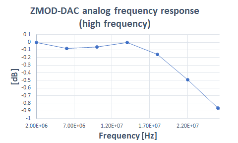
To trace the analog bandwidth of the DAC and output stage beyond the theoretical limit of fSAMPLE/2= 50MHz, the following experiment was performed:
- The AWG was set to generate a 2MHz rectangular signal, 100mV amplitude;
- the theoretical amplitudes of the fundamental and first 69 harmonics was computed;
- the actual amplitudes of the fundamental and first 69 harmonics were measured with a high sampling rate scope (10GSPS, 2GHz BW);
- the dB difference between the theoretical and measured amplitudes was plotted. This represents an approximation of the frequency characteristic of the DAC and output stage.
The characteristic is shown in Fig. 8.
Figure 8. High Frequency AWG spectral characteristics (left), 1dB detail (right)
The 3dB bandwidth is 40MHz+, the 0.5dB bandwidth is 20MHz+, the ±0.1dB flatness band is 14MHz+.
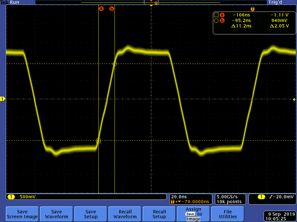
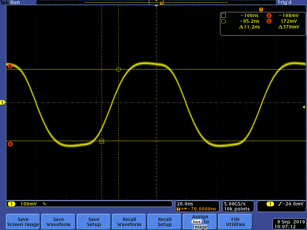
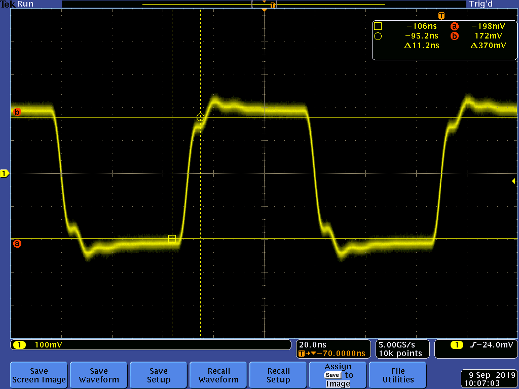
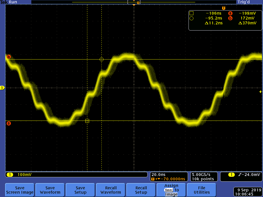
The 3dB bandwidth is close to the theoretical Nyquist limit for a 100MHz sampling system. This has the advantage of very sharp edges (see the rectangular signal in Fig. 9), but also generates alias effects. The Zmod Scope generated signals were recorded with a high BW scope in Fig. 9, and the right side of Fig. 10 and Fig. 11. In Fig. 11, the sinus frequency is 10MHz, and the 100MHz samples are clearly visible. In the left side of Fig. 10 and Fig. 11, the same scope was used, but with 20MHz BW limitation. The rectangular signal edges are slower and the sine wave samples are not visible.
The typical Slew Rate of the AWG can be read in Fig. 9:
$$ SR=\frac{2.05V}{11.2ns}=183V/\mu S \label{18}\tag{18} $$
Figure 9. AWG rectangular signal (large signal)Figure 10. AWG rectangular signal (small signal); scope set at 20MHz BW limit (left), full BW (right)
Figure 11. AWG sinusoidal signal (smallsignal); scope set at 20MHz BW limit (left), full BW (right)
3. MCU
The ATtinny44 MCU works as a I2C memory, storing the SYZYGY™ DNA information and the Calibration Coefficients. The J5 connector is used for programming the MCU and the SYZYGY™ DNA at manufacturing.
The DNA and the Factory Calibration Coefficients are stored in the Flash memory of the MCU, which appears to the I2C interface as “read-only”. The User Calibration Coefficients are stored in the EEPROM memory of the MCU, which is write-protected via a magic number at a magic address. The memory structure can be consulted below.
Figure 12. The MCU
- Program Memory Type: Flash
- Program Memory Size (KB): 4
- CPU Speed (MIPS/DMIPS): 20
- SRAM Bytes: 256
- Data EEPROM/HEF (bytes): 256
- Digital Communication Peripherals: 1-SPI, 1-I2C
- Capture/Compare/PWM Peripherals: 1 Input Capture, 1 CCP, 4PWM
- Timers: 1 x 8-bit, 1 x 16-bit
- Number of Comparators: 1
- Temperature Range (C): -40 to 85
- Operating Voltage Range (V): 1.8 to 5.5
- Pin Count: 14
- Low Power: Yes
Table 1. The Flash memory structure
| Address | Function | Size (Bytes) |
|---|---|---|
| 0x8000 - 0x80FF | DNA | 256 |
| 0x8100 - 0x817F | Factory Calibration | 128 |
| 0x8180 - 0x83FF | Future use | 896 |
3.1. SYZYGY™ DNA
The Zmod AWG is compliant with SYZYGY™ Specification. It contains an MCU able to calculate the Geographical Address and provide the DNA information via I2C. The DNA is stored in the MCU FLASH at the address range: 0x8000 - 0x80FF with the following structure:
Table 2. The Zmod AWG DNA structure
| Contents | Type | Size(Bytes) | Value | Address |
|---|---|---|---|---|
| DNA full data length | uint16 | 2 | 91 | 0x8000 |
| DNA header length | uint16 | 2 | 40 | 0x8002 |
| SYZYGY DNA major version | uint8 | 1 | 1 | 0x8004 |
| SYZYGY DNA minor version | uint8 | 1 | 0 | 0x8005 |
| Required SYZYGY DNA major version | uint8 | 1 | 1 | 0x8006 |
| Required SYZYGY DNA minor version | uint8 | 1 | 0 | 0x8007 |
| Maximum operating 5V load (mA) | uint16 | 2 | 600 | 0x8008 |
| Maximum operating 3.3V load (mA) | uint16 | 2 | 1 | 0x800A |
| Maximum VIO load (mA) | uint16 | 2 | 10 | 0x800C |
| Attribute flags | uint16 | 2 | 0 | 0x800E |
| Minimum operating VIO1 (10 mV steps) | uint16 | 2 | 180 | 0x8010 |
| Maximum operating VIO1 (10 mV steps) | uint16 | 2 | 180 | 0x8012 |
| Minimum operating VIO2 (10 mV steps) | uint16 | 2 | 170 | 0x8014 |
| Maximum operating VIO2 (10 mV steps) | uint16 | 2 | 190 | 0x8016 |
| Minimum operating VIO3 (10 mV steps) | uint16 | 2 | 0 | 0x8018 |
| Maximum operating VIO3 (10 mV steps) | uint16 | 2 | 0 | 0x801A |
| Minimum operating VIO4 (10 mV steps) | uint16 | 2 | 0 | 0x801C |
| Maximum operating VIO4 (10 mV steps) | uint16 | 2 | 0 | 0x801E |
| Manufacturer name length | uint8 | 1 | 12 | 0x8020 |
| Product name length | uint8 | 1 | 13 | 0x8021 |
| Product model / Part number length | uint8 | 1 | 13 | 0x8022 |
| Product version / revision length | uint8 | 1 | 1 | 0x8023 |
| Serial number length | uint8 | 1 | 12 | 0x8024 |
| RESERVED | uint8 | 1 | 0 | 0x8025 |
| CRC-16 (most significant byte) | uint8 | 1 | 0xA5 | 0x8026 |
| CRC-16 (least significant byte) | uint8 | 1 | 0x1E | 0x8027 |
| END DATA HEADER | ||||
| Manufacturer name | string | 12 | Digilent Inc | 0x8028 |
| Product name | string | 13 | Zmod AWG 1411 | 0x8034 |
| Product model / Part number | string | 13 | Zmod AWG 1411 | 0x8041 |
| Product version / revision | string | 1 | C | 0x804E |
| Serial number | string | 12 | 210397000000 | 0x804F |
| Product ID | uint32 | 4 | 0x80200300 | 0x80FC |
3.2. Calibration Memory
The analog circuitry described in previous chapters includes passive and active electronic components. The datasheet specs show parameters (resistance, capacitance, offsets, bias currents, etc.) as typical values and tolerances. The equations in previous chapters consider typical values. Component tolerances affect DC and AC performances of the Zmod AWG. To minimize these effects, the design uses:
- 0.1% resistors and 1% capacitors in all the critical analog signal paths
- Capacitive trimmers for balancing the Scope Input Divider and Gain Selection
- No other mechanical trimmers (as these are big, expensive, unreliable and affected by vibrations, aging, and temperature drifts)
- Software calibration, at manufacturing
- User software calibration, as an option
A software calibration is performed on each device as a part of the manufacturing test. The AWG outputs are connected to calibrated voltmeters. A set of measurements is used to identify all the DC errors (Gain, Offset) of each analog stage. Correction (Calibration) parameters are computed and stored in the Calibration Memory, on the Zmod AWG device, both as Factory Calibration Data and User Calibration Data. The WaveForms software allows the user performing an in-house calibration and overwrite the User Calibration Data. Returning to Factory Calibration is always possible.
The Software reads the calibration parameters from the Zmod AWG MCU via the I2C bus and uses them to correct the generated signals. The structure of the data is shown below:
Table 3. The Calibration Data Structure
| Heading 1 | Name | Size (Bytes) | Type | Flash Address (Factory Calibration) | EEPROM Address (User Calibration) |
|---|---|---|---|---|---|
| Magic ID | 1 | uchar 0xAD | 0x8100 | 0x7000 | |
| Calibration Time | 4 | unix timestamp | 0x8101 | 0x7001 | |
| Channel 1 LG Gain | CG | 4 | float32 | 0x8105 | 0x7005 |
| Channel 1 LG Offset | CA | 4 | float32 | 0x8109 | 0x7009 |
| Channel 1 HG Gain | CG | 4 | float32 | 0x810D | 0x700D |
| Channel 1 HG Offset | CA | 4 | float32 | 0x8111 | 0x7011 |
| Channel 2 LG Gain | CG | 4 | float32 | 0x8115 | 0x7015 |
| Channel 2 LG Offset | CA | 4 | float32 | 0x8119 | 0x7019 |
| Channel 2 HG Gain | CG | 4 | float32 | 0x811D | 0x701D |
| Channel 2 HG Offset | CA | 4 | float32 | 0x8121 | 0x7021 |
| Channel 1 Linearity | 34 | uchar | 0x8125 | 0x7025 | |
| Channel 2 Linearity | 34 | uchar | 0x8147 | 0x7047 | |
| Log | 22 | string | 0x8169 | 0x7069 | |
| CRC | 1 | uchar | 0x817F | 0x707F |
Table 4. The EEPROM Memory Map
| Address | Function | Size (Bytes) |
|---|---|---|
| 0x7000 - 0x707F | User Calibration | 128 |
| 0x7080 - 0x70FF | Future Use | 128 |
At the power up the EEPROM memory is protected against write operations. To disable the write protection one has to write a magic number to a magic address over I2C. To re-enable the write protection one has to write a any other number to the magic address.
Table 5. The Write Protection Disable magic number and address
| Magic Number | Magic Address |
|---|---|
| 0xD2 | 0x6FFF |
4. Power Supplies
This block includes the internal power supplies.
The Zmod AWG gets the digital rails from the carrier board, via the SYZYGY™ connector:
- VCC5V0 - used for relays and analog supplies
- VCC3V3 - used for the MCU and analog supplies
- Vadj = 1.8V - used for the DAC digital rail
The internal analog rails sequence is:
- AVCC3V3 - DAC analog rail, I/V converter (after VCC5V0)
- AVCC-2V5 - I/V converter (after VCC5V0)
- AVCC-8V0, AVCC8V0 - AWG output stage (after VCC3V3)
4.1. AVCC3V3
The analog supply AVCC3V3 is built from VCC5V0 using IC10, an ADP122 5.5 V Input, 300 mA, Low Quiescent Current, CMOS Linear Regulator, Fixed Output Voltage. To reduce noise in the I/V stage, the rail uses the LC filter: FB5 in Fig. 5.
- Input voltage supply range: 2.3 V to 5.5 V
- 300 mA maximum output current
- Fixed and adjustable output voltage versions
- Very low dropout voltage: 85 mV at 300 mA load
- Low quiescent current: 45 µA at no load
- Low shutdown current: <1 µA
- Initial accuracy: ±1% accuracy
- Up to 31 fixed-output voltage options available from 1.75 V to 3.3 V
- Adjustable-output voltage range 0.8 V to 5.0 V (ADP123)
- Excellent PSRR performance: 60 dB at 100 kHz
- Excellent load/line transient response
- Optimized for small 1.0 μF ceramic capacitors
- Current limit and thermal overload protection
- Logic controlled enable
- Compact packages: 5-lead TSOT and 6-lead 2 mm × 2 mm LFCSP
4.2. AVCC-2V5
The AVCC-2V5 analog power supply is implemented with the ADP2301 Step-Down regulator in an inverting Buck-Boost configuration. See application Note AN-1083: Designing an Inverting Buck Boost Using the ADP2300 and ADP2301. To reduce noise and reduce the crosstalk between supplied circuits, the rail uses the LC filter: FB3 in Fig. 5.. The ADP2301 features:
- 1.2 A maximum load current
- ±2% output accuracy over temperature range
- 1.4 MHz switching frequency
- High efficiency up to 91%
- Current-mode control architecture
- Output voltage from 0.8 V to 0.85 × VIN
- Automatic PFM/PWM mode switching
- Integrated high-side MOSFET and bootstrap diode,
- Internal compensation and soft start
- Undervoltage lockout (UVLO), Overcurrent protection (OCP) and thermal shutdown (TSD)
- Available in ultrasmall, 6-lead TSOT package
The output voltage is:
$$V_{OUT}=-V_{FB} \cdot \frac{R_{49}+R_{50}}{R_{50}}=-2.5V\label{19}\tag{19}$$
Where:
$${V_{FB}} = 0.8V\;typical\label{20}\tag{20}$$
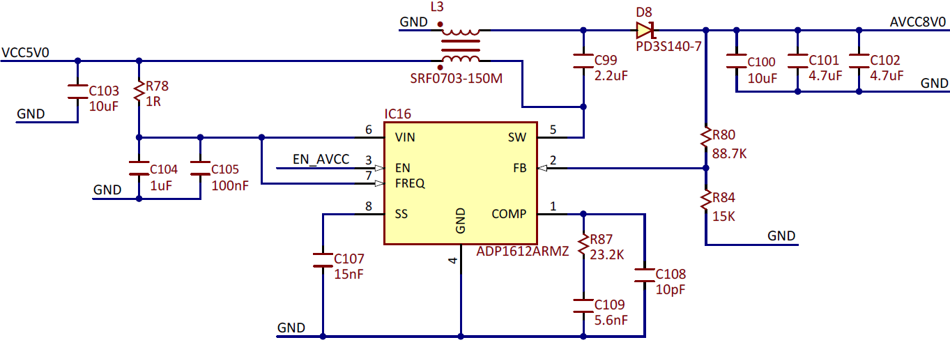
4.3. AVCC8V0
The user power supplies Fig. 15 use ADP1612 Switching Converter in SEPIC DC-to-DC topology. Main features:
- 1.4A current limit
- Minimum input voltage 1.8V
- Pin-selectable 650 kHz or 1.3 MHz PWM frequency
- Adjustable output voltage up to 20 V
- Adjustable soft start
- Undervoltage lockout
The output voltage is:
$$V_{OUT}=V_{FB} \cdot \frac{R_{80}+R_{84}}{R_{84}}=8.538V\label{21}\tag{21}$$
Where:
$${V_{FB}} = 1.235V\;typical\label{22}\tag{22}$$
The supply is enabled after VCC5V0 and AVCC3V3 (see EN_AVCC in Fig. 16)
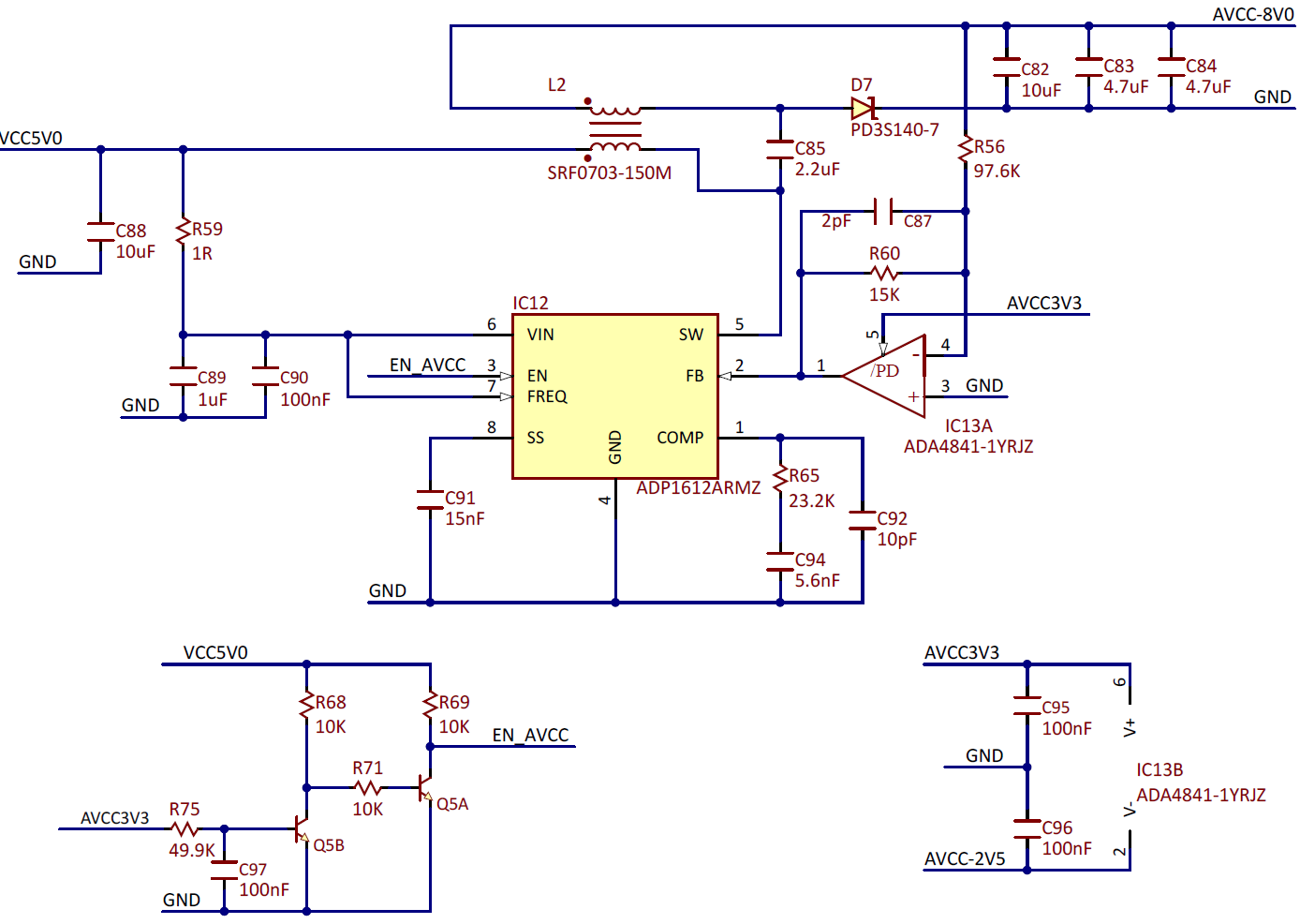
4.4. AVCC-8V0
The user power supplies Fig. 16 use ADP1612 Switching Converter in CUK DC-to-DC topology.
IC13 introduces the required inversion for the negative supply. ADA4841 features:
- Low power: 1.1 mA/amp
- Low wideband noise: 2.1 nV/√Hz, 1.4 pA/√Hz
- Low 1/f noise:7 nV/√Hz @ 10 Hz, 13 pA/√Hz @ 10 Hz
- Low distortion: −105 dBc @ 100 kHz, VO = 2 V p-p
- High speed: 80 MHz, −3 dB bandwidth (G = +1), 12 V/µs slew rate, 175 ns settling time to 0.1%
- Low offset voltage: 0.3 mV maximum
- Rail-to-rail output
- Power down
- Wide supply range: 2.7 V to 12 V
The output voltage is:
$$V_{AVCC8V0}=-V_{FB} \cdot \frac{R_{56}}{R_{60}}=-8.035V\label{23}\tag{23}$$
Where:
$${V_{FB}} = 1.235V\;typical\label{24}\tag{24}$$
The supply is enabled after VCC5V0 and AVCC3V3.
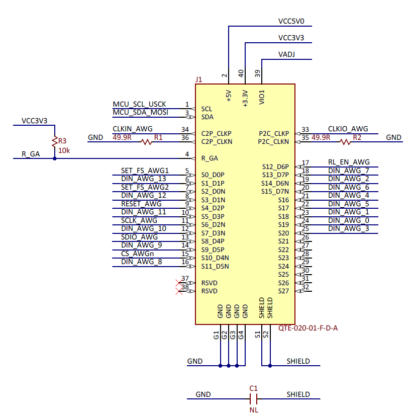
5. The SYZYGY™ Connector
The SYZYGY™ connector in provides the interface with the carrier board. The used signals are:
- Power rails
- VCC5V0
- VCC3V3
- VADJ - needs to be set by the carrier board to 1.8V
- GND
- Shield
- SYZYGY™ I2C bus:
- MCU_SCLUSCK
- MCU_SDA_MOSI
- DAC single ended input clock
- CLKIN_AWG (coupled with GND in the differential C2P pair)
- DAC single ended output clock:
- CLKIO_AWG (coupled with GND in the differential P2C pair)
- R_GA for geographical address identification
- Gain selector signals:
- SET_FS_AWG1
- SET_FS_AWG2
- DAC data bus: DIN_AWG_0…13
- DAC SPI bus:
- CS_SC1n
- SCLK_SC
- SDIO_SC
- relay control
- RL_EN_AWG - enables the AWG outputs
- RESET_AWG
6. The SYZYGY™ compatibility table
Table 6. The SYZYGY™ compatibility table
| Parameter | Value |
|---|---|
| Maximum 5V supply current | 600mA |
| Maximum 3.3V supply current | 1mA |
| VIO supply voltage | 1.8V |
| Maximum VIO supply current | 10mA |
| Total number of I/O | 21 |
| Number of differential I/O pairs | 0 |
| Width | Single |
Written by Mircea Dabacan, PhD, Technical University of Cluj-Napoca Romania


