DMM Shield Reference Manual
The DMM Shield is no longer in production and is retired from the Digilent store. Existing materials will remain available on the DMM Shield Resource Center, but support will be very limited.
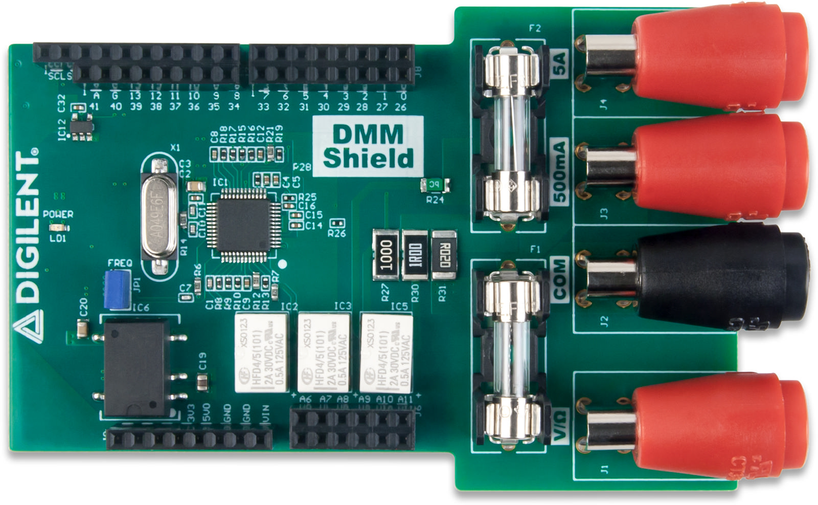
The DMM Shield is a 5 1/2 Digit digital multimeter, designed for use with Digilent microcontroller boards and FPGA boards that are equipped with the Arduino shield header, see Compatible Boards. The shield is built around the HY3131 module from Hycon Technology, which is an analog front end DMM dedicated chip. The device has 7 measurements functions (AC/DC Voltage, AC/DC Current, Resistance, Diode, Continuity) and is factory calibrated. It can be used out of the box with the compatible system boards.
It is accessed through a custom SPI interface, using digital IO pins exposed in the DMM Shield connector.


Overview
Features
- Full compatibility with Digilent System Boards featuring the Arduino Shield
- Provides 4 banana connectors for measurements(Volts/Ω, COM, mAmps, Amps).
- Floating COM
- AC/DC voltage and current measurements
- Diode, continuity measurement/function
- Resistance measurement
- Supports SPI connection
HY3131 Features in Brief
- Programmable multifunctional switch network
- High-resolution, high-speed ∑-Δ ADCs - for high conversion speed, resolution and accuracy
- Digital RMS circuit - the conversion result is processed by the high-speed calculation of the inner hardware to realize the digital RMS [reference: http://www.hycontek.com/wp-content/uploads/Description-HYCON-EN.pdf]
- Operational amplifier
- Multifunctional comparator
- Peak-Hold measurement circuit - to achieve higher accuracy
- Low-Pass filter - implements a third order LPF
- Supports SPI interface connection
Compatible Boards
The DMM Shield is hardware compatible with all Digilent boards that use the Arduino Shield connector, however, the libraries and out of box experience are written for the following boards:
- Arduino Uno
- Arduino Due
- Arduino Mega
The DMMShield can be used with both 3.3V and 5V voltage levels existing on the Arduino boards.
Note: The pic32 library is written to target the uC32 micro-controller board. For all the other boards from the series, the pin-out might suffer modifications.
Specifications
| Voltage and Power Parameters | Min | Typical | Max | Units |
|---|---|---|---|---|
| Power Supply Input Voltage | 3.0 | 3.3 | 3.6 | V |
| Power Supply Input Voltage | - | 5.0 | - | V |
| Power Supply Current Consumption | - | 90 | 100 | mA |
| Ranges | Min | Max | |
|---|---|---|---|
| AC Voltage | -30 | +30 | V |
| DC Voltage | -50 | +50 | V |
| AC/DC Current | -5 | +5 | A |
| Resistances | 50 | 50M | Ω |
- Accuracy: +/-0.1% on Voltage, Current and 500Ω-5MΩ Resistance measurements; +/-1% on 50Ω and 50MΩ Resistances measurements
- Resolution: 5 1/2 Digit
- Floating COM with on board isolated power supply
- Protections:
- 60V PTC for Voltage and resistances and uA
- 630mA fuse for mA rail
- 6.3A fuse for A rail
- Communication: Custom SPI protocol
Power
DMM Shield is powered by the system board. It uses both 5V0 and 3V3 power supplies. The average consumption of the DMM Shield is 90mA. The DMM shield features on-board power supplies that are used to power the DMM core of the board. The 5V power supply is isolated in order to provide an isolated reference signal for measurements. There are more than one reference signals on the DMM Shield board:
- GND - Ground for the non-isolated section. References all the signals and voltage rails in the non-isolated section such as 5V0 and 3V3 voltages from the system board, relay driver, flash memory
- VSS_ISO - Most negative voltage in the isolated section. It is the reference for isolated power supplies VCC5V0_ISO and VCC3V3_ISO as well for all the digital signals in the isolated section
- COM_ISO - Reference for the DMM measurement. All the measurements done with the DMM Shield will be referenced to COM_ISO signal, through COM connector, J2. The reference is leveled at 1.8V above VSS_ISO
- AGND_ISO - Reference for all the analog signals in the isolated section. It is connected to the COM_ISO through a 0Ω resistor
Functional Description
Connectors and Jumpers
The DMM Shield is equipped with the Arduino shield header that provides powering and communication between the DMM Sheild and system board. There are also 4 banana connectors that interface the DMM with the sources and devices that need to be measured.
Banana Connectors (J1-J4)
- J1 (V/Ω) - is used for measuring the AC/DC voltages, Resistances, Diode and Continuity.
- J2 (COM) - is the reference for all the measurements that can be done with the DMM Shield. COM signal is floating from all the other reference points from the board.
- J3 (500mA) - is used for measuring AC/DC currents up to 500mA.
- J4 (5A) - is used for measuring AC/DC currents up to 5A.
Arduino Shield Connector (J5-J9):
- J5 - 1×2 Header - Digital pins
- J6 - 2×6 Header - Analog pins
- J7, J8 - 2×8 Headers - Digital pins
- J9 - 1×8 Header - Power pins
- For detailed usage of each pin please see the Pinout Table Appendix Pinout Table Appendix.
Jumpers:
- JP1 - Frequency Measurement - Not Implemented
Digital Pins Used for Communication
SPI Pins
The DMM Shield supports SPI communication with both the DMM chip and the EEPROM chip. The hardware interface lines DataIn (DI), DataOut (DO) and Clock (CK) are shared between the two devices, and the Chip Select (CS) lines are separate, allowing the user to access either of them with fewer hardware resources used.
The DMM chip is electrically separated from the rest of the circuitry, therefore the communication lines need to be isolated as well.
The EEPROM CS line is active high, while the DMM CS line is active low.
The reading sequence for SPI DMM communication is the one below:
 The writing sequence for SPI DMM communication is the one below:
 The timing for SPI DMM communication is the one below:

GPIO Pins
There are three GPIO pins used for Relay control: RLU, RLD, RLI. Depending on the type of measurement performed, the corresponding relay/s need to be triggered/commanded using a GPIO pin. The relays RLI, RLU, and RLD are controlled by three digital signals, IO2, IO3, and IO4, from the shield connector.
| Scales | RLI | RLU | RLD |
|---|---|---|---|
| 50MΩ | 0 | 0 | 1 |
| 5MΩ | 0 | 0 | 1 |
| 500kΩ | 0 | 0 | 1 |
| 50kΩ | 0 | 0 | 1 |
| 5kΩ | 0 | 0 | 1 |
| 500Ω | 0 | 0 | 1 |
| 50Ω | 0 | 0 | 1 |
| 50VDC | 0 | 1 | 0 |
| 5VDC | 0 | 1 | 0 |
| 500mVDC | 0 | 0 | 1 |
| 50mVDC | 0 | 0 | 1 |
| 50VAC | 0 | 1 | 0 |
| 5VAC | 0 | 1 | 0 |
| 500mVAC | 0 | 0 | 1 |
| 50mVAC | 0 | 0 | 1 |
| 5ADC | 0 | 0 | 0 |
| 500mADC | 0 | 0 | 0 |
| 50mADC | 0 | 0 | 0 |
| 5mADC | 1 | 0 | 0 |
| 500uADC | 1 | 0 | 0 |
| 5AAC | 0 | 0 | 0 |
| 500mAAC | 0 | 0 | 0 |
| 50mAAC | 0 | 0 | 0 |
| 5mAAC | 1 | 0 | 0 |
| 500uAAC | 1 | 0 | 0 |
| Continuity | 0 | 0 | 1 |
| Diode | 0 | 0 | 1 |
In addition to configuring the GPIO pins, setting each scale assumes the configuration of some registers. The HY3131 chip provides 23 configurable registers.
| Scales | INTE | R20 | R21 | R22 | R23 | R24 | R25 | R26 | R27 | R28 | R29 | R2A | R2B | R2C | R2D | R2E | R2F | R30 | R31 | R32 | R33 | R34 | R35 | R36 |
|---|---|---|---|---|---|---|---|---|---|---|---|---|---|---|---|---|---|---|---|---|---|---|---|---|
| 50MΩ | 0x00 | 0xC0 | 0xCF | 0x17 | 0x93 | 0x85 | 0x00 | 0x00 | 0x55 | 0x55 | 0x00 | 0x00 | 0x08 | 0x00 | 0x00 | 0x80 | 0x86 | 0x80 | 0xD1 | 0x3C | 0xA0 | 0x00 | 0x00 | 0x00 |
| 5MΩ | 0x00 | 0xC0 | 0xCF | 0x17 | 0x93 | 0x85 | 0x00 | 0x00 | 0x55 | 0x55 | 0x00 | 0x00 | 0x08 | 0x00 | 0x80 | 0x80 | 0x86 | 0x80 | 0xD1 | 0x3C | 0xA0 | 0x00 | 0x00 | 0x00 |
| 500kΩ | 0x00 | 0xC0 | 0xCF | 0x17 | 0x93 | 0x85 | 0x00 | 0x00 | 0x55 | 0x55 | 0x00 | 0x00 | 0x08 | 0x00 | 0x08 | 0x80 | 0x86 | 0x80 | 0xD1 | 0x33 | 0x20 | 0x00 | 0x00 | 0x00 |
| 50kΩ | 0x00 | 0xC0 | 0xCF | 0x17 | 0x83 | 0x85 | 0x00 | 0x00 | 0x55 | 0x00 | 0x00 | 0x00 | 0x40 | 0x00 | 0x06 | 0x44 | 0x94 | 0x80 | 0xD3 | 0x33 | 0x20 | 0x00 | 0x00 | 0x00 |
| 5kΩ | 0x00 | 0xC0 | 0xCF | 0x17 | 0x83 | 0x85 | 0x00 | 0x00 | 0x55 | 0x00 | 0x00 | 0x00 | 0x40 | 0x60 | 0x00 | 0x44 | 0x94 | 0x80 | 0xD3 | 0x33 | 0x20 | 0x00 | 0x00 | 0x00 |
| 500Ω | 0x00 | 0xC0 | 0xCF | 0x17 | 0x83 | 0x35 | 0x00 | 0x00 | 0x55 | 0x00 | 0x00 | 0x00 | 0x40 | 0x06 | 0x00 | 0x44 | 0x94 | 0x80 | 0xD2 | 0x3C | 0xA0 | 0x00 | 0x00 | 0x00 |
| 50Ω | 0x00 | 0xC0 | 0xCF | 0x17 | 0x83 | 0x35 | 0x01 | 0x00 | 0x55 | 0x00 | 0x00 | 0x00 | 0x40 | 0x06 | 0x00 | 0x44 | 0x94 | 0x80 | 0xD2 | 0x3C | 0xA0 | 0x00 | 0x00 | 0x00 |
| 50VDC | 0x00 | 0x60 | 0x00 | 0x17 | 0x8B | 0x01 | 0x11 | 0x00 | 0x55 | 0x31 | 0x00 | 0x22 | 0x00 | 0x00 | 0x09 | 0x28 | 0xA0 | 0x80 | 0xC7 | 0x33 | 0x20 | 0x00 | 0x00 | 0x00 |
| 5VDC | 0x00 | 0x60 | 0x00 | 0x17 | 0x8B | 0x01 | 0x11 | 0x00 | 0x55 | 0x31 | 0x00 | 0x22 | 0x00 | 0x00 | 0x90 | 0x28 | 0xA0 | 0x80 | 0xC7 | 0x33 | 0x20 | 0x00 | 0x00 | 0x00 |
| 500mVDC | 0x00 | 0xC0 | 0x00 | 0x17 | 0x8B | 0x85 | 0x11 | 0x00 | 0x55 | 0x31 | 0x00 | 0x00 | 0x00 | 0x00 | 0x00 | 0x00 | 0x90 | 0x80 | 0xC7 | 0x33 | 0x28 | 0x00 | 0x00 | 0x00 |
| 50mVDC | 0x00 | 0x00 | 0x00 | 0x17 | 0x8B | 0x35 | 0x11 | 0x00 | 0x55 | 0x31 | 0x00 | 0x00 | 0x00 | 0x00 | 0x00 | 0x00 | 0x90 | 0x80 | 0xC7 | 0x3C | 0x60 | 0x00 | 0x00 | 0x00 |
| 50VAC | 0x00 | 0xF2 | 0xDD | 0x07 | 0x03 | 0x52 | 0x10 | 0x80 | 0x25 | 0x31 | 0xF8 | 0x22 | 0x00 | 0x00 | 0x0D | 0x28 | 0xA0 | 0xFF | 0xC7 | 0x38 | 0x20 | 0x00 | 0x00 | 0x00 |
| 5VAC | 0x00 | 0xF2 | 0xDD | 0x07 | 0x03 | 0x52 | 0x10 | 0x80 | 0x25 | 0x31 | 0xF8 | 0x22 | 0x00 | 0x00 | 0xD0 | 0x88 | 0xA0 | 0xFF | 0xC7 | 0x38 | 0x20 | 0x02 | 0x50 | 0x0C |
| 500mVAC | 0x00 | 0x92 | 0xDD | 0x07 | 0x03 | 0x52 | 0x10 | 0x80 | 0x25 | 0x11 | 0xF8 | 0x00 | 0x00 | 0x00 | 0x00 | 0x00 | 0x90 | 0x80 | 0xC7 | 0x3A | 0x28 | 0x00 | 0x00 | 0x00 |
| 50mVAC | 0x00 | 0x52 | 0xDD | 0x07 | 0x03 | 0x00 | 0x13 | 0x80 | 0x25 | 0x11 | 0xF8 | 0x00 | 0x00 | 0x00 | 0x00 | 0x00 | 0x90 | 0x80 | 0xC7 | 0x3A | 0x28 | 0x00 | 0x00 | 0x00 |
| 5ADC | 0x00 | 0x00 | 0x00 | 0x17 | 0x8B | 0x95 | 0x11 | 0x00 | 0x55 | 0x31 | 0x00 | 0x00 | 0x00 | 0x00 | 0x00 | 0x00 | 0x80 | 0x80 | 0xC7 | 0x33 | 0x20 | 0x00 | 0x00 | 0x00 |
| 500mADC | 0x00 | 0x00 | 0x00 | 0x17 | 0x8B | 0x95 | 0x11 | 0x00 | 0x55 | 0x31 | 0x00 | 0x00 | 0x00 | 0x00 | 0x00 | 0x00 | 0x80 | 0x80 | 0xC7 | 0x33 | 0xA0 | 0x00 | 0x00 | 0x00 |
| 50mADC | 0x00 | 0x00 | 0x00 | 0x17 | 0x8B | 0x35 | 0x11 | 0x00 | 0x55 | 0x31 | 0x00 | 0x00 | 0x00 | 0x00 | 0x00 | 0x00 | 0x80 | 0x80 | 0xC7 | 0x3D | 0x20 | 0x00 | 0x00 | 0x00 |
| 5mADC | 0x00 | 0x00 | 0x00 | 0x17 | 0x8B | 0x95 | 0x11 | 0x00 | 0x55 | 0x31 | 0x00 | 0x00 | 0x00 | 0x00 | 0x00 | 0x00 | 0x80 | 0x80 | 0xC7 | 0x33 | 0x20 | 0x00 | 0x00 | 0x00 |
| 500uADC | 0x00 | 0x00 | 0x00 | 0x17 | 0x8B | 0x35 | 0x11 | 0x00 | 0x55 | 0x31 | 0x00 | 0x00 | 0x00 | 0x00 | 0x00 | 0x00 | 0x80 | 0x80 | 0xC7 | 0x3D | 0xA0 | 0x00 | 0x00 | 0x00 |
| 5AAC | 0x00 | 0x52 | 0xDD | 0x07 | 0x03 | 0x00 | 0x13 | 0x80 | 0x25 | 0x11 | 0xF8 | 0x00 | 0x00 | 0x00 | 0x00 | 0x00 | 0x90 | 0x80 | 0xC7 | 0x3D | 0x28 | 0x00 | 0x00 | 0x00 |
| 500mAAC | 0x00 | 0x92 | 0xDD | 0x07 | 0x03 | 0x52 | 0x10 | 0x80 | 0x25 | 0x11 | 0xF8 | 0x00 | 0x00 | 0x00 | 0x00 | 0x00 | 0x90 | 0x80 | 0xC7 | 0x3D | 0x28 | 0x00 | 0x00 | 0x00 |
| 50mAAC | 0x00 | 0x52 | 0xDD | 0x07 | 0x03 | 0x00 | 0x13 | 0x80 | 0x25 | 0x11 | 0xF8 | 0x00 | 0x00 | 0x00 | 0x00 | 0x00 | 0x90 | 0x80 | 0xC7 | 0x3D | 0x28 | 0x00 | 0x00 | 0x00 |
| 5mAAC | 0x00 | 0x92 | 0xDD | 0x07 | 0x03 | 0x52 | 0x10 | 0x80 | 0x25 | 0x11 | 0xF8 | 0x00 | 0x00 | 0x00 | 0x00 | 0x00 | 0x90 | 0x80 | 0xC7 | 0x3D | 0x28 | 0x00 | 0x00 | 0x00 |
| 500uAAC | 0x00 | 0x52 | 0xDD | 0x07 | 0x03 | 0x00 | 0x13 | 0x80 | 0x25 | 0x11 | 0xF8 | 0x00 | 0x00 | 0x00 | 0x00 | 0x00 | 0x90 | 0x80 | 0xC7 | 0x3D | 0x28 | 0x00 | 0x00 | 0x00 |
| Continuity | 0x00 | 0x74 | 0xCF | 0x17 | 0x83 | 0x35 | 0x10 | 0x00 | 0x55 | 0x00 | 0x00 | 0x00 | 0x00 | 0x0A | 0x00 | 0x40 | 0x86 | 0x80 | 0xD2 | 0x3C | 0xA0 | 0x00 | 0x00 | 0x00 |
| Diode | 0x00 | 0xC0 | 0xCF | 0x17 | 0x8B | 0x8D | 0x10 | 0x00 | 0x55 | 0x31 | 0x00 | 0x00 | 0x00 | 0x08 | 0x00 | 0x40 | 0x86 | 0x80 | 0xE2 | 0x33 | 0xA0 | 0x00 | 0x00 | 0x00 |
For more information please see the library documentation for each platform ZYNQ or Digilent Microcontroller boards.
EEPROM Memory
The DMM Shield is equipped with a non-volatile EEPROM memory chip from Microchip: 93LC66BT datasheet available from Microchip's website ), which has 512 bytes/256 words (4kbits) available space. The memory can be accessed over a custom SPI protocol, using digital IO pins exposed in the DMM Shield connector: CS_EEPROM (EEPROM SPI chip select), DO (SPI MISO), DI (SPI MOSI) and CLK (SPI CLK).
While the chip select line is specific to EEPROM module, the SPI lines (data and clock) are shared with the DMM device.
Note the data is written and read from memory using word format addressing, instead of byte: bytes 0-1 are written at address 0x00, bytes 2-3 are written at address 0x01, etc.
The EEPROM is used to store the following system information:
| Section Content | Addresses (words) | Size |
|---|---|---|
| Factory calibration data | 0x93 – 0xFF | 109 words / 218 bytes |
| Serial Number | 0x8C – 0x92 | 7 words / 14 bytes |
| User calibration data | 0x1F – 0x8B | 109 words / 218 bytes |
| Free Memory | 0x00 – 0x1E | 31 words / 62 bytes |
Please consult the DMM Shield Library User Guide for more information about the EEPROM module usage and communication. For more details about Calibration process, read more on Calibration Procedure below.
Measurement Scales
DMM Shield comes with preset scales of measurement. They will indicate the maximum value that can be accurately measured with the device. Keep in mind that at low values the resolution is lower and different scales might give a more accurate result since the device is calibrated closer that value. Ex: for a 40kΩ resistor is better to use the 50kΩ scale instead of the 500kΩ for a better resolution. There are 4 scales for voltages, 5 for current and 7 for resistances. Additionally, there are two extra scales for Diode and Continuity.
| Scales | - | - | - | - | - | - | - | - |
|---|---|---|---|---|---|---|---|---|
| AC Voltage | 50m | 500m | 5 | 30 | - | - | - | V |
| DC Voltage | 50m | 500m | 5 | 50 | - | - | - | V |
| AC/DC Current | 500u | 5m | 50m | 500m | 5 | - | - | A |
| Resistances | 50 | 500 | 5k | 50k | 500k | 5M | 50M | Ω |
| Diode | ||||||||
| Continuity |
The device comes factory calibrated for each scale. For more details about calibration please see the Calibration procedure below.
Accuracy
The accuracy of the DMM Shield is around 0.1% for AC/DC Currents and Voltages, 500Ω-5MΩ Resistances and within the scales; 1% for 50Ω and 50MΩ Resistances. For AC Current and Voltage we guarantee the 0.1% accuracy at 50/60Hz. Note that outrunning the end of a scale will increase the measurement error. The accuracy is computed in percentage as a difference between the reference value and the measured value, reported to full scale.
Let's consider $R_{F}, M_{F}$ as the reference and the measured value at full scale and $F_{S}$ the full scale. The accuracy is computed as follows:
$$Accuracy=\frac {R_{F} - M_{F}}{F_{S}} * 100\label{10}\tag{10}$$
Calibration Procedure
The DMMShield needs calibration before performing measurements and delivering correctly measured values to the user. This is due to errors introduced by the chip itself and on-board additional electronics. Calibration is the process of computing and applying correction coefficients to the measured values that allow precise measurements.
The process consists of computing an additive and a multiplicative coefficient for each scale.
Calibration is done by collecting pairs of reference value and measured value (RefVal, MsVal) in multiple points. The reference value is the value measured with an accurate instrument, considered to be the actual value to be measured by the DMMShield device. The measured value is the value reported by DMMShield hardware. When all these pairs are collected, the calibration coefficients are computed mainly using the difference between the reference and the measured values.
Depending on the scale, different types of calibration are performed, as detailed in the following chapters:
2 Points Calibration for Resistance Scales
This method applies to the Resistance scales. It collects the pairs (RefVal, MsVal) in two points: 0 point (short between probes), and full scale value.
Let’s consider this pairs as being ($R_{0}$, $M_{0}$) and ($R_{F}$, $M_{F}$). The calibration coefficients are computed in the following manner:
$$Calib_{MULT}=\frac {R_{0} - R_{F}}{M_{0} - M_{F}} - 1\label{1}\tag{1}$$ $$Calib_{ADD}=(R_{0} - M_{0})(1 + Calib_{MULT})\label{2}\tag{2}$$
The reference value for the short is considered to be 0: $R_{0} = 0$
The calibration coefficients are applied to the acquired value in the following manner: $$Value_{corrected}=(1 + Calib_{MULT})Value_{acquired} + Calib_{ADD}\label{3}\tag{3}$$
3 Points Calibration for DC
This method applies to the DC Voltage and DC Current scales. It collects the pairs (RefVal, MsVal) in three points: 0 point (short between probes for voltage and open for current), negative full scale value and positive full scale value. For example, for VoltageDC500m scale, the following points are used: 0 point (short between probes), -500mV, 500 mV.
Let’s consider this pairs as being ($R_{0}$, $M_{0}$), ($R_{FN}$, $M_{FN}$) and ($R_{FP}$, $M_{FP}$). The calibration coefficients are computed in the following manner:
$$Calib_{MULT}=\frac {R_{FP} - R_{FN}}{M_{FP} - M_{FN}} - 1\label{4}\tag{4}$$ $$Calib_{ADD}=(R_{0} - M_{0})(1 + Calib_{MULT})\label{5}\tag{5}$$
The reference value for the zero calibration is considered to be 0: $R_{0} = 0$
The calibration coefficients are applied to the acquired value in the following manner: $$Value_{corrected}=(1 + Calib_{MULT})Value_{acquired} + Calib_{ADD}\label{6}\tag{6}$$
2 Points Calibration for AC
This method applies to the AC Voltage and AC Current scales. It collects the pairs (RefVal, MsVal) in two points: 0 point (short between probes for voltage and open for current) and full scale value. For example, for VoltageAC500m scale, the following points are used: 0 point (short between probes) and 500 mV.
Let’s consider this pairs as being ($R_{0}$, $M_{0}$), ($R_{F}$, $M_{F}$). The calibration coefficients are computed in the following manner: $$Calib_{MULT}=\frac {R_{F}}{\sqrt{{M_{F}}^2 - {M_{0}}^2}} - 1\label{7}\tag{7}$$ $$Calib_{ADD}= M_{0}\label{8}\tag{8}$$
The reference value for the zero calibration is considered to be 0: $R_{0} = 0$
The calibration coefficients are applied to the acquired value in the following manner: $$Value_{corrected}=(1 + Calib_{MULT})\sqrt{| {Value_{acquired}}^2- {Calib_{ADD}}^2 |}\label{9}\tag{9}$$
Software Libraries
Digilent provides libraries to access DMM Shield functionality. The libraries were created to support ZYNQ plaform and Digilent PIC32 microcontroller boards. Both libraries come with a demo that allows the communication with the DMM Shield through UART. Functions as setting a scale and measure can be accessed by entering commands in the UART terminal emulator. Another demo shows how to access the memory left in the EEPROM by reading and writing 32 words. Documentation and downloads for these libraries can be found at the following locations:
Appendix: Pinout Tables
DMM Shield Connector Pinout
Banana Connector Interface
| J1 | J2 | J3 | J4 |
|---|---|---|---|
| Voltage/Ω | COM | Current (mA) | Current (A) |
Power Connector
| J9 | |
| Connector pin number | Arduino Shield Name |
|---|---|
| 1 | NC |
| 2 | 3V3 |
| 3 | NC |
| 4 | 3V3 |
| 5 | 5V0 |
| 6 | GND |
| 7 | GND |
| 8 | VIN |
Analog Connector
| J6 | |||
| Outer Row | Inner Row | ||
| Connector pin number | Arduino Shield Name | Connector pin number | Arduino Shield Name |
|---|---|---|---|
| 1 | A0 | 2 | A6 |
| 3 | A1 | 4 | A7 |
| 5 | A2 | 6 | A8 |
| 7 | A3 | 8 | A9 |
| 9 | A4 | 10 | A10 |
| 11 | A5 | 12 | A11 |
Digital IO Connector
| J7 | |||
| Inner Row | Outer row | ||
| Connector pin number | Arduino Shield Name | Connector pin number | Arduino Shield Name |
|---|---|---|---|
| 1 | IO41 | 2 | A |
| 3 | IO40 | 4 | G |
| 5 | IO39 | 6 | IO13/CLK |
| 7 | IO38 | 8 | IO12/DI |
| 9 | IO37 | 10 | IO11/DO |
| 11 | IO36 | 12 | IO10/CS_DMM |
| 13 | IO35 | 14 | IO9/CS_EEPROM |
| 15 | IO34 | 16 | IO8 |
| J8 | |||
| Inner Row | Outer Row | ||
| Connector pin number | Arduino Shield Name | Connector pin number | Arduino Shield Name |
| 1 | IO33 | 2 | IO7 |
| 3 | IO32 | 4 | IO6 |
| 5 | IO31 | 6 | IO5 |
| 7 | IO30 | 8 | IO4/RLD |
| 9 | IO29 | 10 | IO3/RLU |
| 11 | IO28 | 12 | IO2/RLI |
| 13 | IO27 | 14 | IO1 |
| 15 | IO26 | 16 | IO0 |
About this Document
This reference manual applies to Revision C of the DMM Shield.