Nexys 4 - Getting Started with Microblaze Servers
Warning!
This guide is out of date. While it should still work as written in the original versions of the tools it was written for, users have reported that resulting designs are not functional in recent versions - 2022.2 being the latest at time of writing.

Overview
This guide will provide a step by step walk-through of creating a Microblaze based hardware design using the Vivado IP Integrator that will build over the Getting Started with Microblaze guide by making use of the on-board Ethernet port and GPIOs for the Nexys 4 FPGA board.
At the end of this tutorial you will have a comprehensive hardware design for Nexys4 that makes use of various Hardware ports on the Nexys 4 which are managed by the Microblaze Softcore Processor block.
Prerequisites
Software
- Xilinx Vivado with the SDK package
Board Support Files
- Board Support Files. These files will describe GPIO interfaces on your board and make it easier to select your FPGA board and add GPIO IP blocks.
- Follow this Wiki guide (Vivado Board Files for Digilent 7-Series FPGA Boards ) on how to install Board Support Files for Vivado 2014.4
Hardware
- Digilent Nexys 4 FPGA Board and Micro USB Cable for UART communication and JTAG programming
Tutorial
Microblaze is a soft IP core from Xilinx that will implement a microprocessor entirely within the Xilinx FPGA general purpose memory and logic fabric. For this tutorial, we are going to add Ethernet functionality and create an echo server.
General Design Flow
I. Vivado
* Open Vivado and select Nexys 4 board
* Create an new Vivado Project
* Create empty block design workspace inside the new project
* Add required IP blocks using the IP integrator tool and build Hardware Design
* Validate and save block design
* Create HDL system wrapper
* Run design Synthesis and Implementation
* Generate Bit File
* Export Hardware Design including the generated bit stream file to SDK tool
* Launch SDK
Now the Hardware design is exported to the SDK tool. The Vivado to SDK hand-off is done internally through Vivado. We will use SDK to create a Software application that will use the customized board interface data and FPGA hardware configuration by importing the hardware design information from Vivado.
II. SDK
* Create new application project and select default Hello World template
* Program FPGA
* Run configuration by selecting the correct UART COM Port and Baud Rate
1. Create a new project
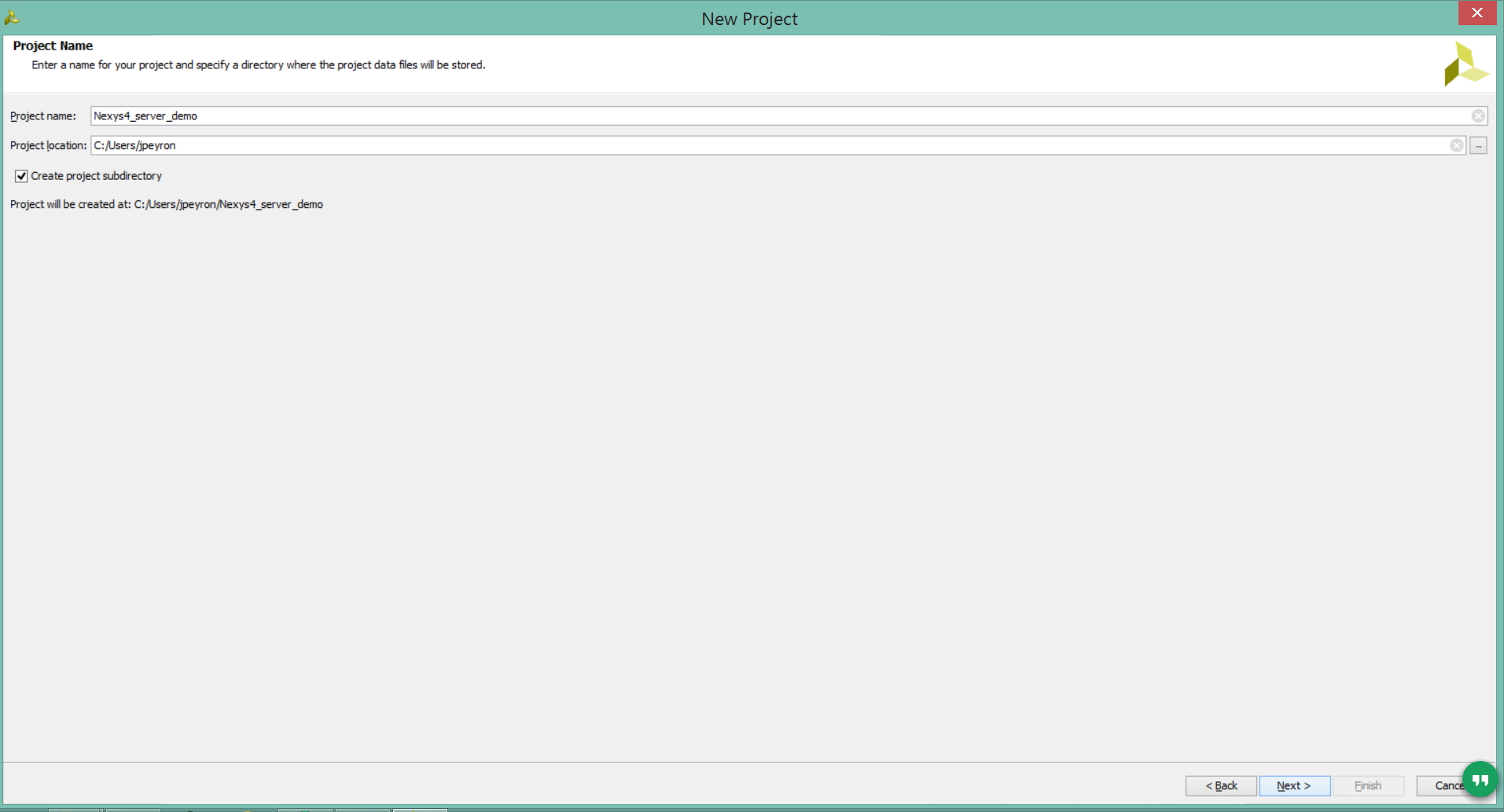
1.1) Click on Create New Project. Choose the Project Name and Location such that there are no blank spaces. This is an important naming convention to follow for project names, file names and location paths.
Underscore in a good substitute for empty spaces.
It is good practice to have a dedicated folder for Vivado Projects, preferably with the smallest possible path length. Example: C:/Vivado_Projects.
Name your Project and select the Project location and click next.
1.2) Choose Project Type as RTL Project. Leave the - do not specify sources box unchecked and click next.

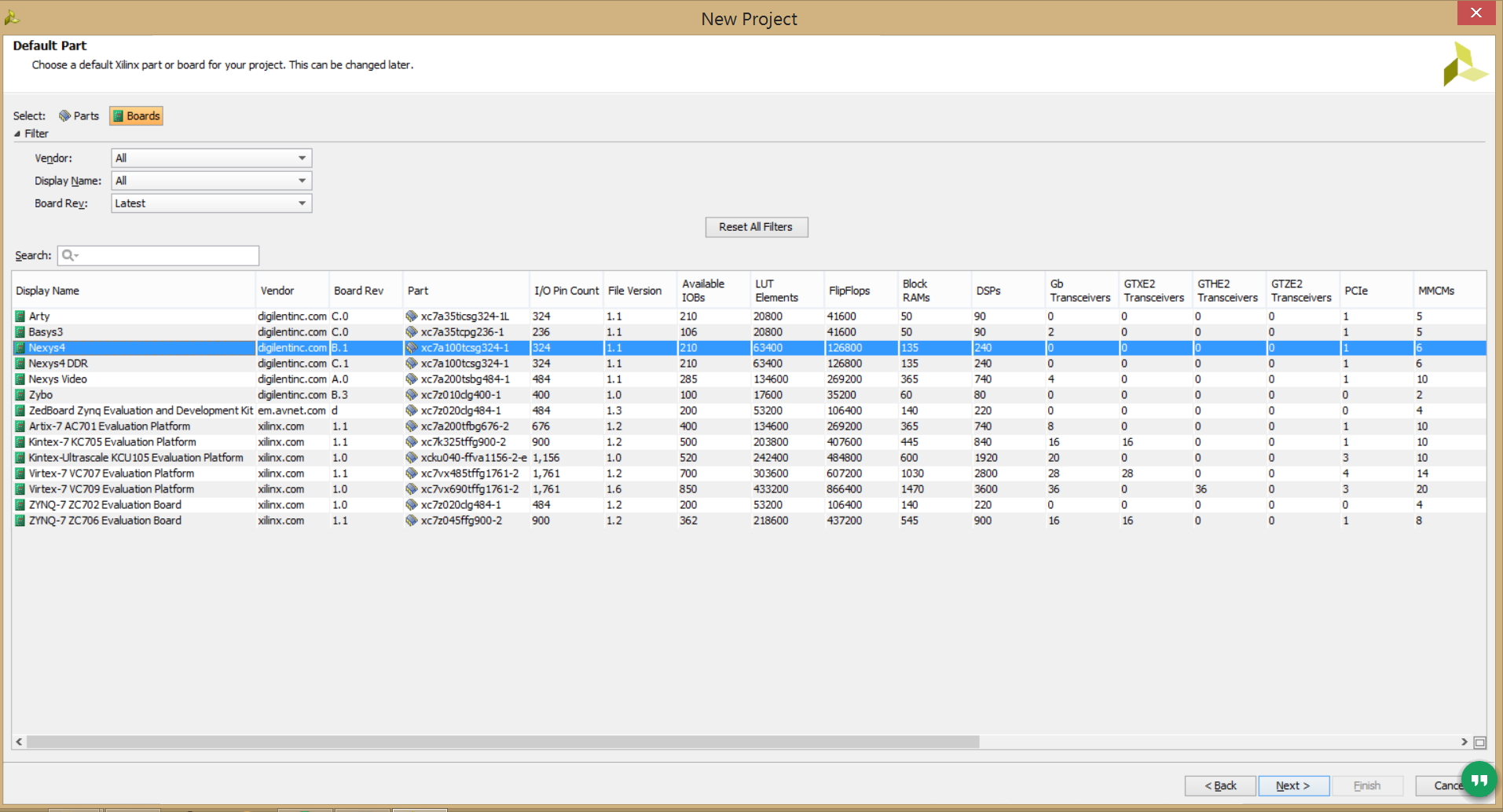
1.3) If you have followed the Board Support File Wiki guide then click next and select Boards.
From the filter options make required selections for Vendor, Display Name and Board Revision.
Nexys 4 should be displayed in the selection list. A mismatch in selecting the correct board name will cause errors.
1.4) Click Next, followed by Finish and Vivado will create a project for you.
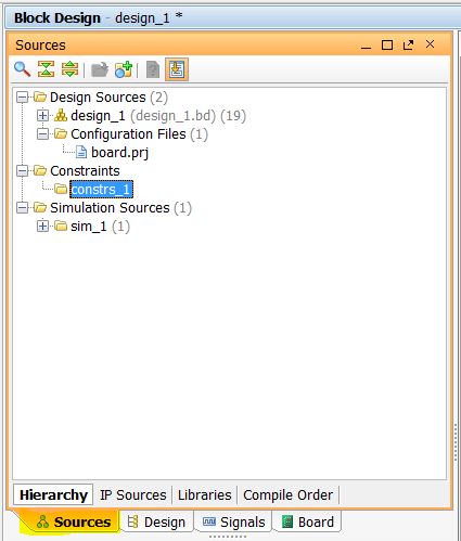
2. Create a Block Design
2.1) Create a Block Design by clicking the button circled in blue below.

3. Add the Microblaze Core
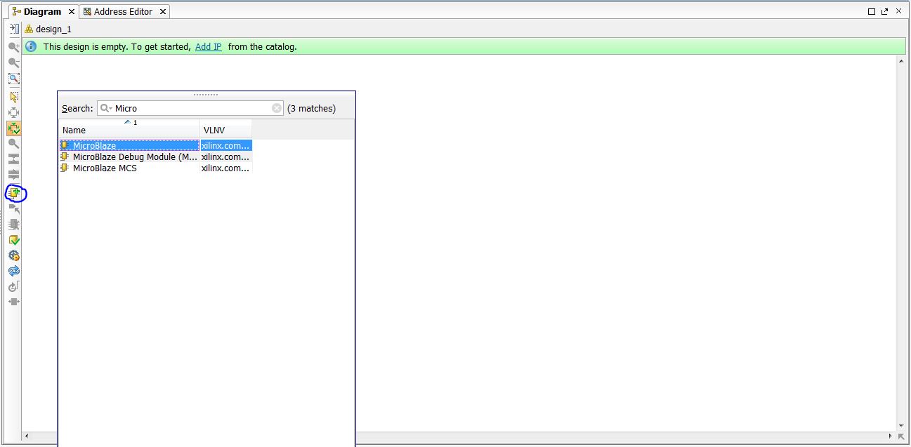
3.1) Start out by clicking the “Add IP” button circled in blue below. Search for “Microblaze” and double click the IP highlighted below.
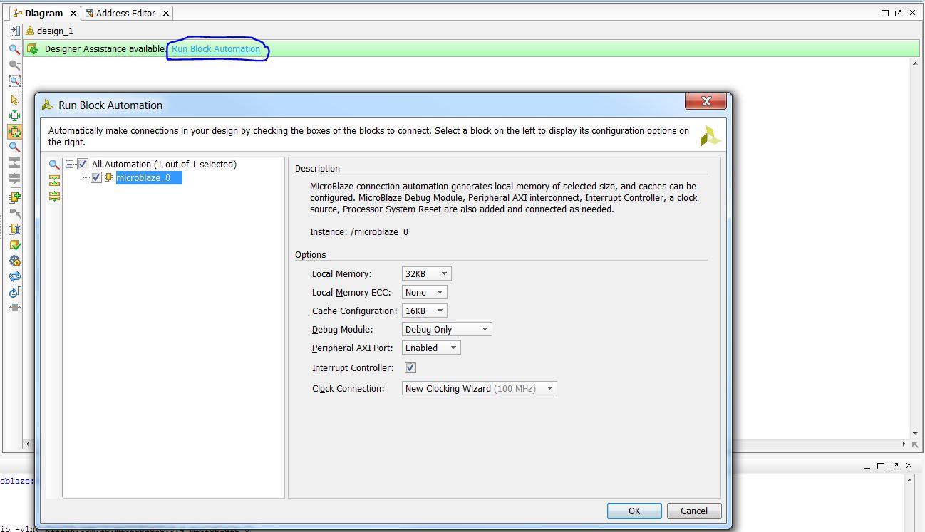
3.2) Click “Run Block Automation” circled in blue, and change the options to match the ones in the picture below. Click “Ok”.
4. Adding the Necessary Output Clocks
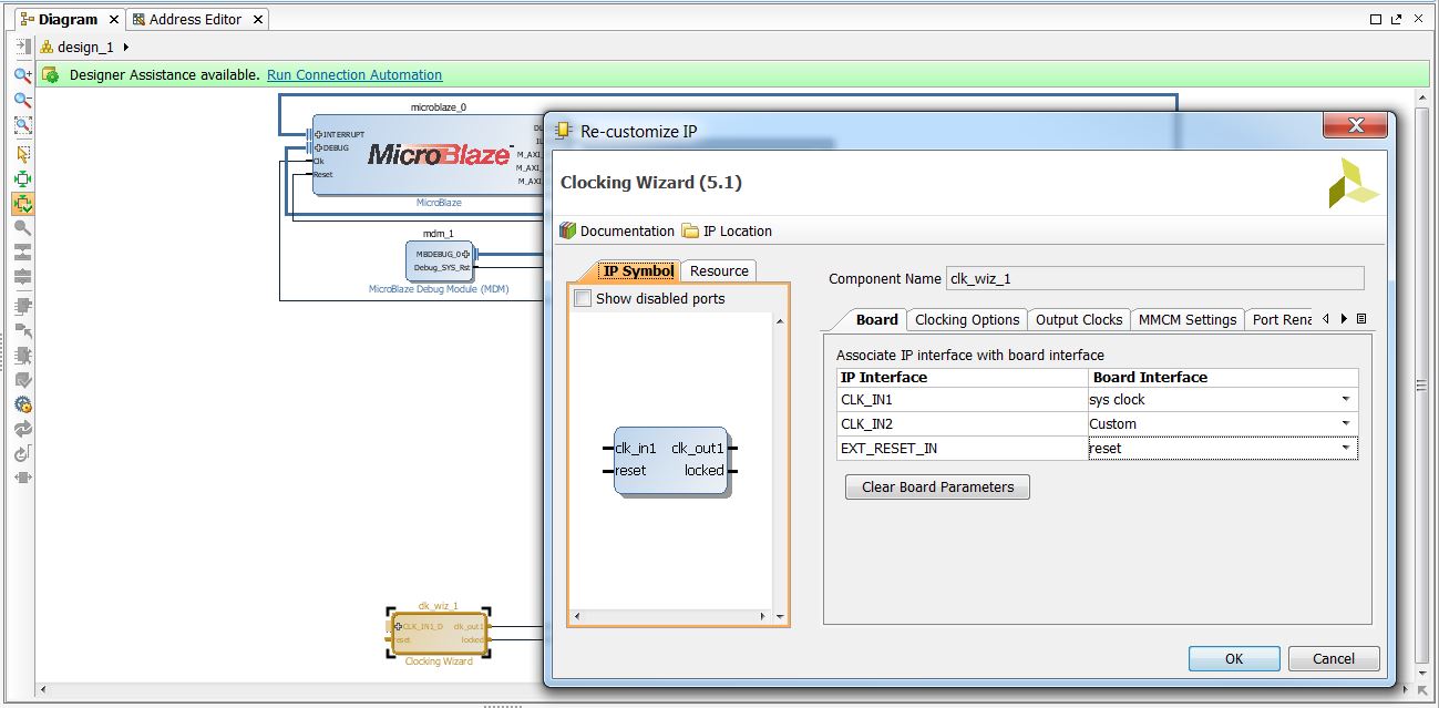
4.1) Double-click the Clocking Wizard block highlighted below, and set CLK_IN1 to use “sys_clock” and EXT_RESET_IN to use “reset”.
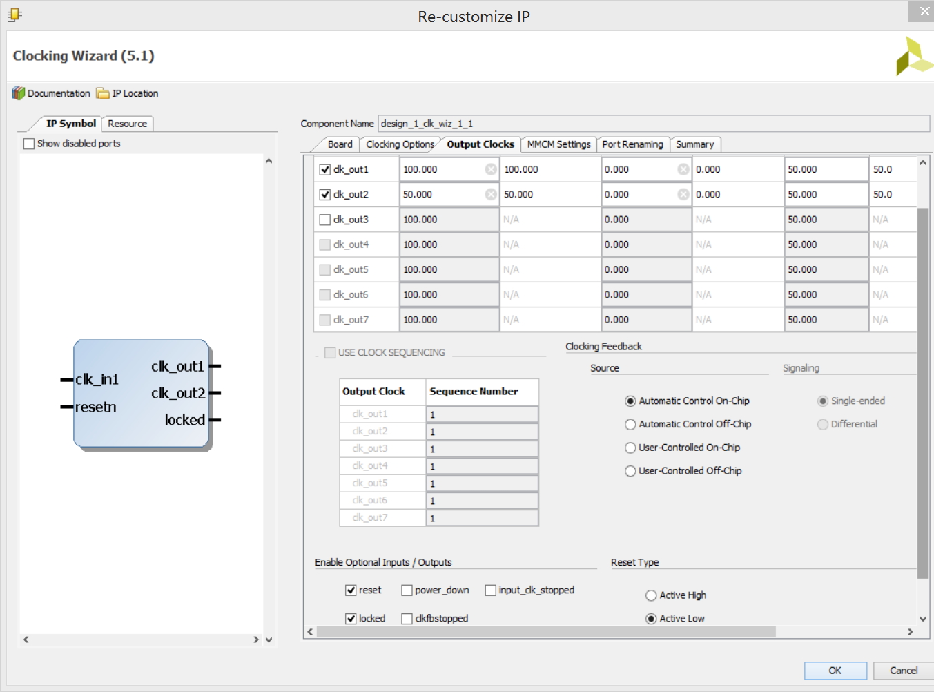
4.2) Select the Output Clocks tab and enable clk_out2. Set clk_out2 to 50MHz. These will clock the memory controller and the Ethernet Reference clock, respectively.
Set the Reset Type to Active Low using the bullets below. When you are finished, click Ok.
Your block design should look something like this:

5. Adding the IP Cores
5.1) We will now add all of the necessary IP blocks to our project. There are 5 cores we will add:
* AXI EMC
* AXI Uartlite
* Ethernet PHY MII to Reduced MII
* AXI EthernetLite
* AXI Timer
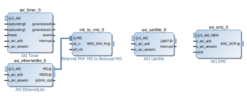
Add all of these to your design, one at a time, using the “Add IP” button. Once they are all added, you should see the five blocks shown below.
6. Configuring and Routing the IP Cores
6.1) On the AXI EMC block, connect the rdlk input to the clk1 output on the Clock wizard block. To do this, hover over the blue rectangle next to EMC rdclk until you see a pencil cursor. Click and drag this over to the clk1 output of the other block and release.
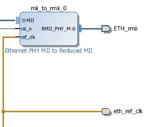
6.2) On the AXI EthernetLite block, connect the MII output to the MII input on the Ethernet PHY MII to Reduced MII block. To do this, hover over the blue rectangle next to MII+ until you see a pencil cursor. Click and drag this over to the +MII input of the other block and release.
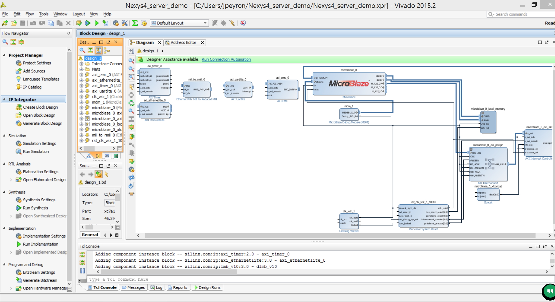
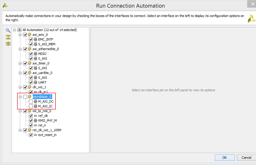
6.3) Click “Run Connection Automation”. Un-check the microblaze_0 check-box and click OK.
6.4) Click Regenerate Layout (circled in blue below), and your block design should look like this:

6.5)
* Route interrupt on the AXI Timer block to In0[0:0] on the Concat block.
* Route ip2intc_irpt on the AXI EthernetLite block to In1[0:0] on the Concat block.
* Connect resetn on the Clocking Wizard block to the reset pin.


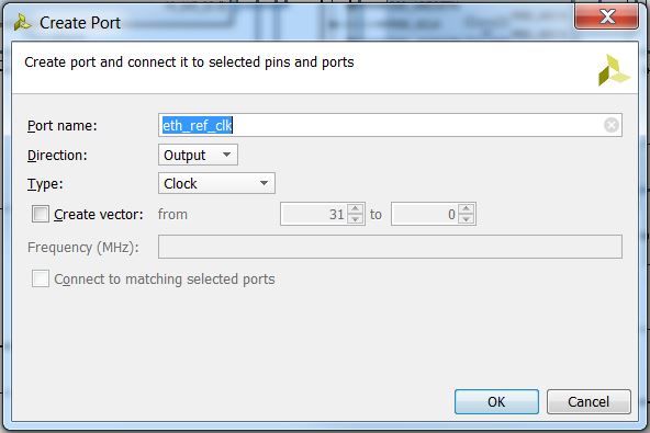
6.6) Right click somewhere in the background (white space) of your design and click Create Port…, or use the shortcut, Ctrl-K. Name this port eth_ref_clk and change the options to the one in the picture below.
6.7) Connect this eth_ref_clk pin to ref_clk on the Ethernet PHY MII to Reducted MII block. Then Connect both to the output pin clk_out2 from the clock wizard.
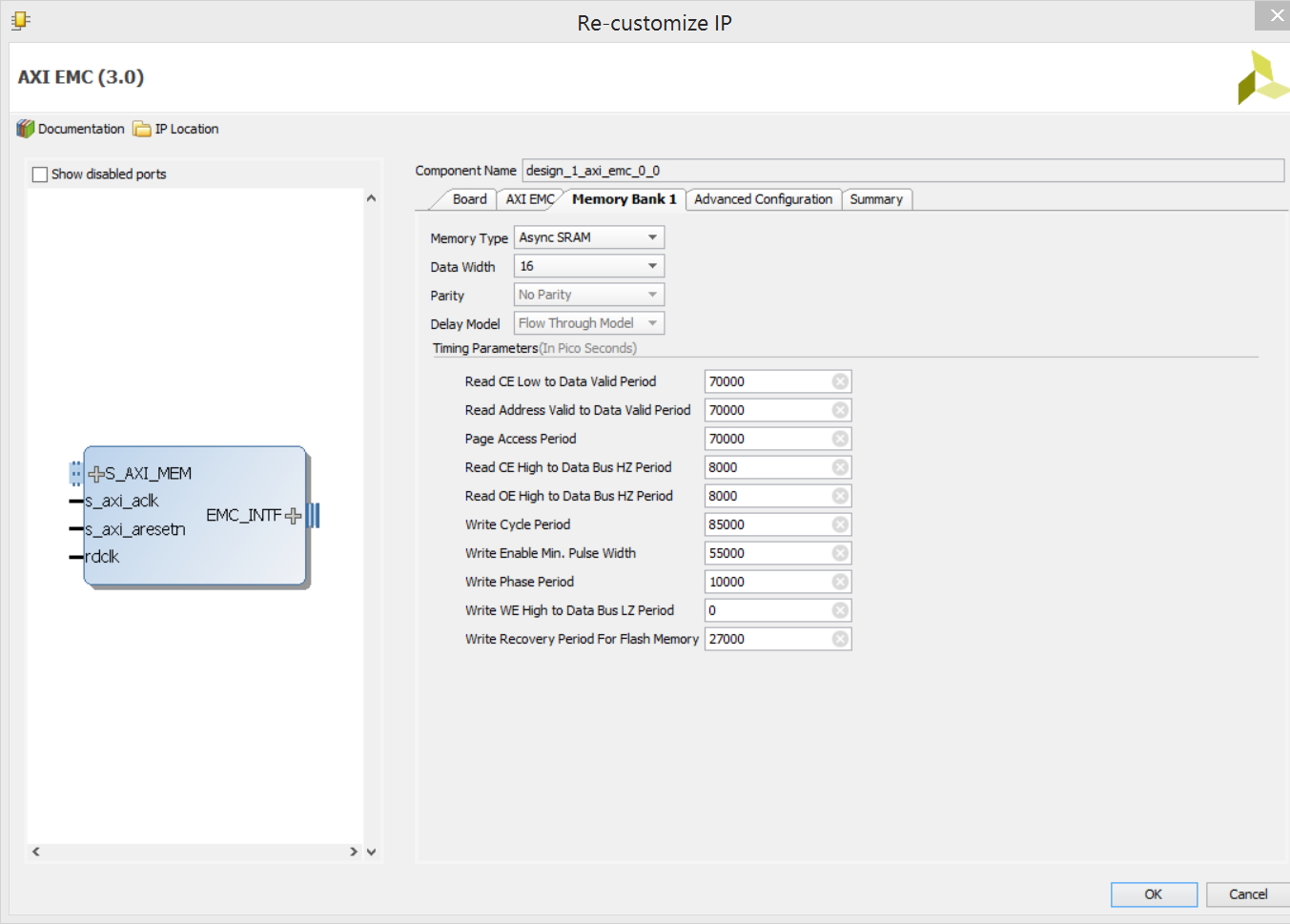
6.8) Double click into the AXI EMC block, select Memory Bank1, settings are as seen below.
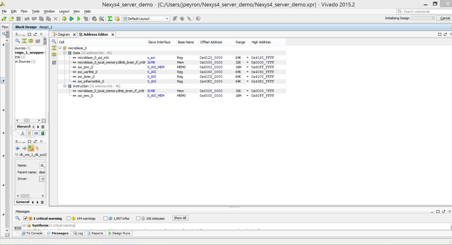
6.9) click on the Address Edditor select both S_AXI_MEM and change the range to 16M.
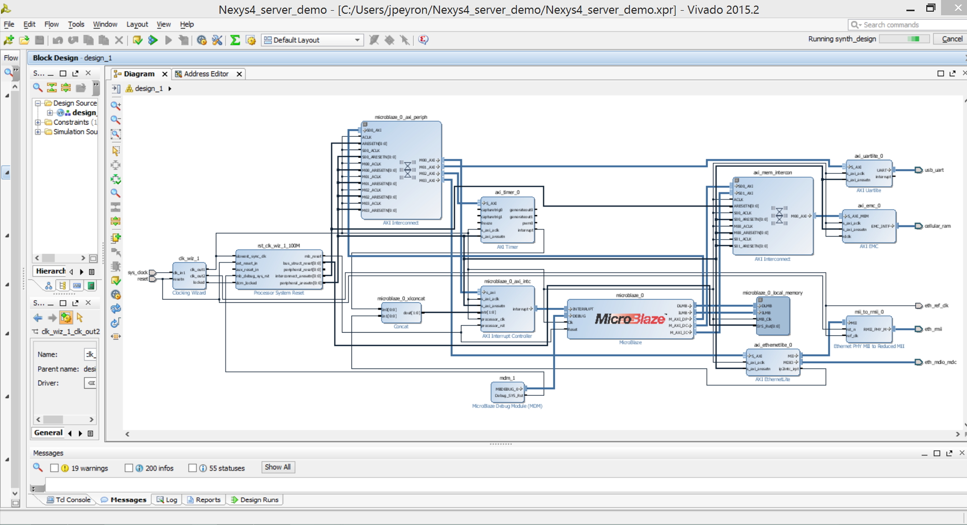
6.10) Clicking Regenerate Layout again will result in your final block design layout for this project.
6.11) We must now connect the eth_ref_clk pin to the correct pin on the FPGA by creating an XDC file. Under the Design window, select the Sources tab. Expand the contraints folder, right click on constr and click “Add Sources…”
6.12) Select Add or create constraints and click Next.

6.13) Click Create File…, name your new contraints file and click OK and then Finish.

6.14) Open your new constraints file and paste the following line of code in it:
set_property -dict { PACKAGE_PIN D5 IOSTANDARD LVCMOS33 } [get_ports { eth_ref_clk }];
Save the xdc file when you are finished.
6.15) Now, right click on your design_1 block diagram and click “Create HDL Wrapper”. When the window pops up, select the “Let Vivado manage wrapper and auto-update” bullet and click OK.

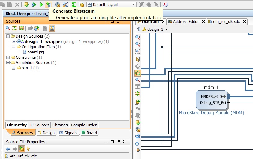
6.16) Click “Generate Bitstream” at the top of the work space. This process will take a while.
7. Exporting Hardware Design to SDK
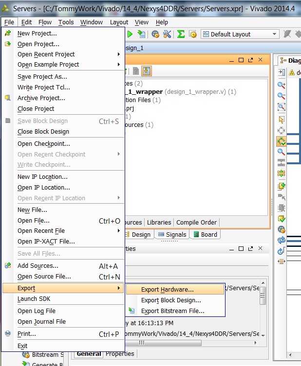
7.1) On the top left corner of the window, from the tool bar click on File and select Export Hardware.
This will export the hardware design with system wrapper for the Software Development Tool - Vivado SDK.
Make sure the generated bitstream is included by checking the box.
8. Launching SDK
8.1) Go to File and select Launch SDK and click OK. The SDK file created local to the Vivado design project location will be launched. The hand-off to SDK from Vivado is complete.

9. Inside SDK for Vivado
9.1) A new window for SDK will open. The HW design specification and included IP blocks are displayed in the system.hdf file. SDK tool is independent of Vivado, i.e. from this point, you can create your SW project in C/C++ on top of the exported HW design. If necessary, you can also launch SDK directly from the SDK folder created in the main Vivado Project directory.
Now, if you need to go back to Vivado and make changes to the HW design, then it is recommended to close the SDK window and make the required HW design edits in Vivado. After this you must follow the sequence of creating a new HDL wrapper, save design and bit file generation. This new bit file and system wrapper must then be exported to SDK.
Since we do not have any HW design edits at this point, we will proceed with creating a software application to run an echo server.

10. Creating New Application Project in SDK
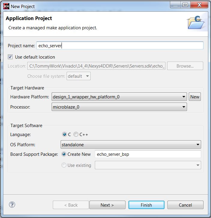
10.1) Go to File in the main tool bar and select New » Application Project. A new project window will pop up.
Give your SDK project a name that has no empty spaces as shown below. Make sure the Target Hardware is the correct hardware design. In our case, it will be “design_1_wrapper_hw_platform_0”.
If for example, you also have another hardware design in the Project Explorer window, then you will also see this design name in the Target Hardware drop down selection list.
Since we only have one hardware design design_1_wrapper_hw_platform_0 this will be our target hardware. Select Create New under Board Support Package. The tool will automatically populate the Board Support Package name to match with the give project name.
Click Next.
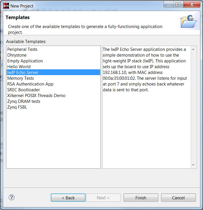
Select IwIP Echo Server under the list of available templates and click Finish.
10.2) After completing the previous step, you will see two new folders in the Project Explorer panel.
echo_server which contains all the binaries, .C and .H (Header) files
echo_server_bsp which is the board support folder
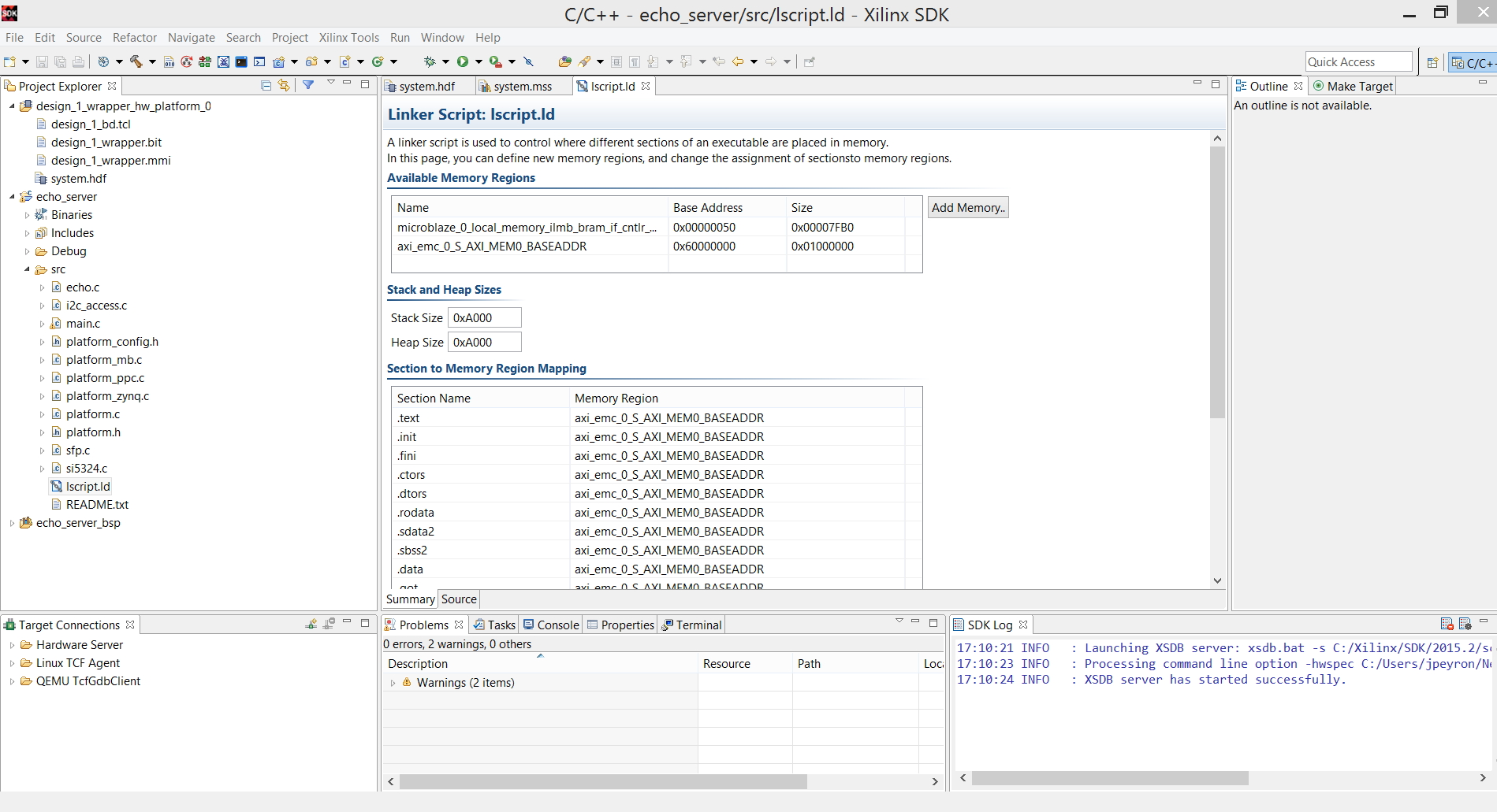
echo_server is our main working source folder. This also contains an important file shown here in the src folder called “lscript.ld”. This is a Xilinx auto generated linker script file. Double click on this file to open.
11. Verify Linker Script File for Memory Region Mapping
11.1) In the linker script, take a look at the Available Memory Regions box. The Name should be axi_emc_0_s_AXI_MEMO_BASEADDR and the Size should be 0x01000000
12. Setting PHY Link Speed
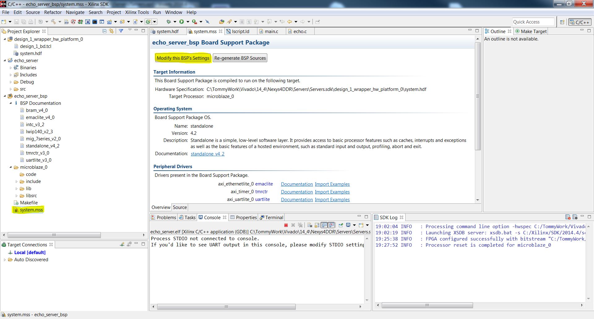
12.1) Open the system.mss file within the echo_server_bsp folder and click Modify this BSP's Settings.
Select lwip140, then expand the temac_adapter_options and find phy_link_speed in the list. Change the value of phy_link_speed to CONFIG_LINKSPEED100 and press OK.

13. Programming FPGA with Bit File
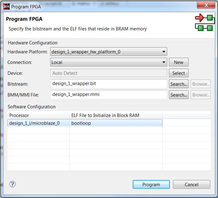
13.1) Make sure that the Nexys 4 DDR is turned on and connected to the host PC with the provided micro USB cable. On the main toolbar, click Xilinx Tools»Program FPGA
Make sure that the Hardware Platform is selected as design_1_wrapper_hw_platform_0.
In the software configuration box, under ELF File to Initialize in Block RAM column, the row option must read bootloop. If not, click on the row and select bootloop.
Now click on Program.
14. Setting up the SDK Serial Console and Running the Server
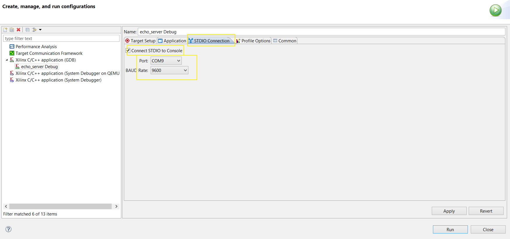
14.1) Right click on the echo_server project folder and select Run As » Run Configurations
Go to the STDIO Connection tab and check the Connect STDIO to Console check-box. Click Apply, then click Run.

15. Running the Server
15.1) In the console window at the bottom of the screen the details of the connection will be displayed.

16. Testing the Server with Tera Term
16.1) Connect your PC to your Nexys4 using an Ethernet cable.
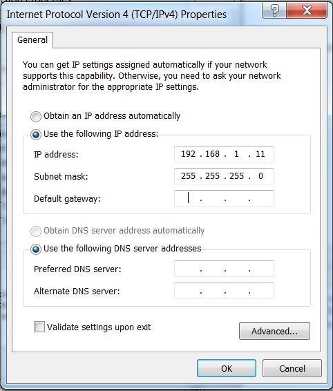
16.2) In order to connect to the echo server, you must set up your Ethernet connection with a static IP address.
To do this:
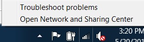
* Right click your internet connection and click Open Network and Sharing Center.
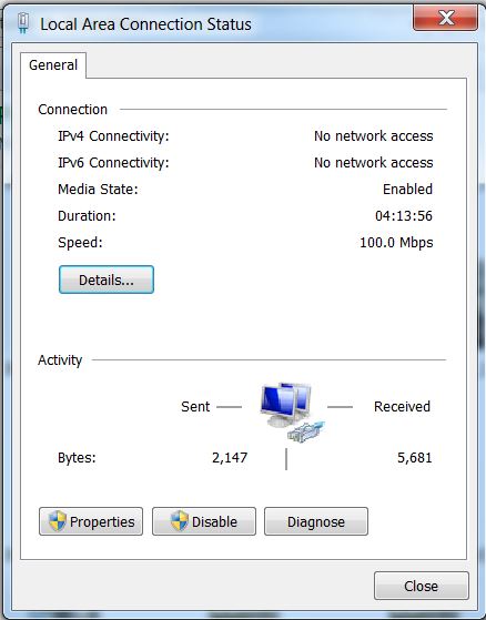
* Find the Ethernet Connection to your Nexys4-DDR. It should be an unidentified network. Click Local Area Connection.
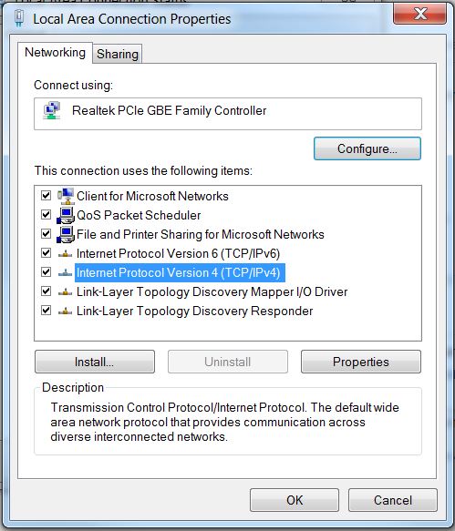
* Click Properties.
* Select Internet Protocol Version 4 (TCP/IPv4) and click Properties.
* Click the Use the following IP address: bullet and type in an IP address 192.168.1.XX, where XX is a value between 2 and 255, but not 10. Make sure to click within the Subnet mask field to get the 255.255.255.0 mask to autofill. Click Ok and you will have a static IP address.

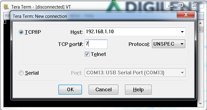
16.3) Open Tera Term and type in the following info and click Ok.
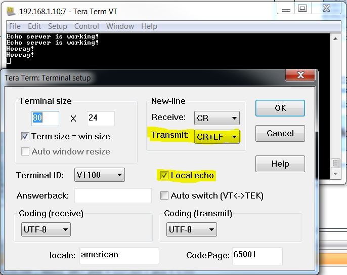
16.4) Type anything into the console and press Enter. The echo server will echo back your input and display it in the console.
You can go to Setup>Terminal and change the settings below for a more traditional echo server format