Getting Started with ARTY's Base System Design

Overview
This guide will provide a step by step walk-through of opening the Arty Base System Design Project in Vivado and getting started in Xilinx SDK.
At the end of this tutorial you will have:
- Opened the pre-made Microblaze based hardware ( HW ) design in Xilinx Vivado.
- Imported and implemented a custom DigiLEDs IP block into the design.
- Created .C Project in Xilinx Vivado SDK ( Software Development Kit) to interface with the Arty.
Prerequisites
Skills
- Familiarity with Vivado
- Block Design Experience
Hardware
- Digilent Arty FPGA Board
- Micro USB Cable
- Used for UART communication and JTAG programming
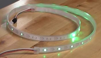
- Programmable RGB LEDs (WS2812, Neopixels)
- Data-in Signal wire connected to ARTY's JB1
Software
- Xilinx Vivado 2015.3 or 2015.4 with the SDK package.
- Follow this Wiki guide (Installing Vivado ) on how to install and activate Vivado
Board Support Files
- Arty Support Files
- These files will describe GPIO interfaces on your board and make it easier to select your FPGA board and add GPIO IP blocks.
- Follow this Wiki guide (Vivado Board Files for Digilent 7-Series FPGA Boards ) on how to install Board Support Files for Vivado.
Project Files
- Arty BSD Tutorial Files : ZIP
Introduction
The Arty Base System Design is a pre-made project that routes all of the necessary hardware on the Arty to the Microblaze processor to be used in Xilinx SDK. This allows the user to jump straight into software design in SDK.
In this tutorial, we are going to add our own custom IP block into the base system design to be used with some programmable RGB LEDs.
General Design Flow
I. Vivado
- Open Vivado
- Execute the BSD tcl script to import the project
- Add the DigiLEDs custom IP to the project's IP repository
- Add the DigiLEDs IP to the design and configure it.
- Validate and save block design
- Create HDL system wrapper
- Run design Synthesis and Implementation
- Generate Bit File
- Export Hardware Design including the generated bit stream file to SDK tool
- Launch SDK
Now the Hardware design is exported to the SDK tool. The Vivado to SDK hand-off is done internally through Vivado. We will use SDK to create a Software application that will use the customized board interface data and FPGA hardware configuration by importing the hardware design information from Vivado.
II. SDK
- Create new application project and select Empty Application template
- Import main.c
- Program FPGA
Tutorial
1. Creating a New Project
1.1) Download and extract the project files to a directory you will remember. We will used “C:/Work” for this tutorial.
1.2) Open up Vivado and find the tcl Console on the bottom of the screen.

1.2) Type “cd C:/Work/BSD/proj” in the tcl console. This will move you to the folder that contains the tcl script that will generate the BSD project.
1.3) Type “source ./create_project” in the tcl console. This will automatically generate the BSD project.
When it is done, you should see the Arty Base System Design shown below.

2. Adding Our Custom IP Repo
2.1) Find and click “Project Settings” under Project Manager on the left side of Vivado.

2.2) Within project settings, click “IP” on the left side. Then click the “Repository Manager” tab and click the + button (Highlighted below).

2.3) Navigate to your projects folder and select the “DigiLED-master” folder.

2.4) Verify that the new repo is in the list and click OK to exit project settings.

3. Adding Our Custom IP
3.1) Click the “Add IP” button highlighted below.

3.2) Type “DigiLED” in the search box and double click “DigiLED_v1.0”. This will add our custom IP to the block design.

3.3) Click “Run Connection Automation” and click “OK” to connect the IP to Microblaze.

4. Configuring the IP
4.1) Find the DigiLED_0 block and double click the block to customize it.

4.2) Select the HSV Bullet and change the Number of LEDs field to the number of LEDs on your RGB LED strip before clicking OK.

5. Adding the LED Signal Pin
5.1) Right click within your block design and click “Create Port”

5.2) Name the port “led_pin” and set it as an Output. Click OK.

5.3) Connect the “led_pin” to “led_out” on the DigiLED_0 block using your cursor (It will look like a pencil).

5.4) On the left of your block design, select the Sources tab, and open the pins.xdc file within the Constraints folder.

5.5) Copy the line below, and paste it within pins.xdc. This is the pin connected to Connector JB1.
set_property -dict { PACKAGE_PIN E15 IOSTANDARD LVCMOS33 } [get_ports { led_pin }]; #IO_L11P_T1_SRCC_15 Sch=jb_p[1]
5.6) Save pins.xdc and close it.
6. Deleting/Creating HDL System Wrapper
6.1) Within the Sources tab, click “system_wrapper - STRUCTURE” and press Delete. You can also right on it and click “Remove file from Project”. Check the box and click OK.

6.2) In the next window that pops up, click “Ignore and continue with invalid top module” and click OK.

6.3) Right click system.bd and click Create HDL Wrapper…

7. Generating Bit File
7.1) In the top toolbar, click Generate Bitstream. If you haven't already saved your design, you will get a prompt to save the block design.

7.2) After the bitstream has been generated, a message prompt will pop-up on the screen. You don't have to open the Implemented Design for this demo. Just click on Cancel.

8. Exporting Hardware Design to SDK
8.1) On the top left corner of the window, from the tool bar click on File and select Export Hardware.
This will export the hardware design with system wrapper for the Software Development Tool - Vivado SDK.
Make sure the generated bitstream is included by checking the box.

9. Launching SDK
9.1) Go to File and select Launch SDK and click OK. The SDK file created local to the Vivado design project location will be launched. The hand-off to SDK from Vivado is complete.

10. Inside SDK for Vivado
10.1) A new window for SDK will open. The HW design specification and included IP blocks are displayed in the system.hdf file. SDK tool is independent of Vivado, i.e. from this point, you can create your SW project in C/C++ on top of the exported HW design. If necessary, you can also launch SDK directly from the SDK folder created in the main Vivado Project directory.
Now, if you need to go back to Vivado and make changes to the HW design, then it is recommended to close the SDK window and make the required HW design edits in Vivado. After this you must follow the sequence of creating a new HDL wrapper, save design and bit file generation. This new bit file and system wrapper must then be exported to SDK.
Since we do not have any HW design edits at this point, we will proceed with creating a software application.

10.2) On the left corner of the main SDK window, you will find the Project Explorer panel. Notice that there is a main project folder under the name system_wrapper_hw_platform_0.
system is the name of your block design created in Vivado. This hardware platform has all the HW design definitions, IP interfaces that have been added, external output signal information and local memory address information.
Say if at this point, you have closed SDK, made edits to your existing hardware design, and exported your design to SDK then after launching the SDK tool, you will find a new hardware platform called: system_wrapper_hw_platform_1 in addition to the old HW design i.e. system_wrapper_hw_platform_0.

11. Creating New Application Project in SDK
11.1) Go to File in the main tool bar and select New Application Project. A new project window will pop up.
Give your SDK project a name that has no empty spaces such as “DigiLEDs”. Make sure the Target Hardware is the correct hardware design. In our case, it will be “system_wrapper_hw_platform_0”. Click “Next”.

11.2) Select Empty Application under Available Templates on the left panel and click Finish.
11.3) After completing the previous step, you will see two new folders in the Project Explorer panel.**DigiLEDs** which contains all the binaries, .C and .H (Header) files **DigiLEDs_bsp** which is the board support folderDigiLEDs is our main working source folder. This also contains an important file shown here which is the “lscript.ld”. This is a Xilinx auto generated linker script file.


12. Adding the Main Source File
12.1) Navigate to your project files folder within the Work directory and find the “main.c” file.
12.2) Click and drag this main.c file into the DigiLEDs/src folder within Xilinx SDK. Choose to copy these source files into the project and click OK.

13. Programming FPGA with Bit File
13.1) Make sure that the Arty is turned on and connected to the host PC with the provided micro USB cable.
In the quick selection tool bar, you will find a symbol with a red arrow and three green square boxes.
Click on this symbol to open the Program FPGA window.
Make sure that the Hardware Platform is selected as system_wrapper_hw_platform_0.
In the software configuration box, under ELF File to Initialize in Block RAM column, the row option must read bootloop. If not, click on the row and select bootloop.
Now click on Program.


14. Program the Microblaze Processor
14.1) After the FPGA has been successfully programmed with the bit file, from the Project Explorer panel, right click on the “DigiLEDs” project folder. Go to “Run As” and select “Launch on Hardware (System Debugger)“
Your Arty will then start the DigiLEDs Demo. Pressing Button 0 will cycle through three patterns on the RGB LED strip.

—-