Getting Started with Vivado for Hardware-Only Designs
Introduction

The goal of this guide is to familiarize the reader with the Vivado tools through the “Hello World!” of hardware, blinking an LED.
Note: While this guide was originally created using Vivado 2016.4, the workflow described has not substantially changed, and the guide works as described through to Vivado 2022.1, the latest version as of the time of writing.
Prerequisites
Prior to starting this guide make sure to install Vivado:
- For versions 2019.2 and later, see Installing Vivado, Vitis, and Digilent Board Files.
- For versions prior to 2019.2, see Installing Vivado, Xilinx SDK, and Digilent Board Files.
- Download digilent-xdc-master.zip and extract it to a disk drive folder for later use.
Guide
Launch Vivado
Select the dropdown corresponding to your operating system, below.
- Windows
-
Open Vivado through the start menu or desktop shortcut created during the installation process.


- Linux
-
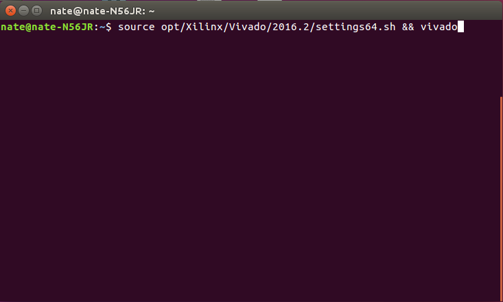
Open a terminal, and change directory (cd) to a folder where log files for your Vivado session can be placed, then run the following commands:
source <install_path>/Vivado/<version>/settings64.sh
vivado

Create a Vivado Project
In Vivado's welcome screen, several options are presented:
- Create Project: Opens a wizard used to begin creating a Vivado project from scratch, which will be used here.
- Open Project: Can be used to open a Vivado project (defined by an XPR file) that has been previously created or downloaded from the internet.
- Open Hardware Manager: Can be used to program an FPGA development board with a bitstream, without opening the associated project.
Note: Various other options are available, but are not described here.
For the purposes of this guide, click the Create Project button.

The first page of the New Project wizard summarizes the steps involved in creating a project. Click Next.

The first step is to set the name for the project. Vivado will use this name when generating its folder structure.
Important: Do NOT use spaces in the project name or location path. This will cause problems with Vivado. Instead use an underscore, a dash, or CamelCase.
Pick a memorable location in your filesystem to place the project.
Checking the Create project subdirectory box will create a new folder in the chosen location to store the project's files. This is recommended.
Click Next to continue.

At the Select Project Type screen, choose RTL Project and check the Do not specify sources at this time box. Advanced users may want to use the other options on this screen, but they will not be covered here.
Click Next to continue.

Next, a part or a board must be chosen for the project to target. The project will only be usable with the chosen device (though the selection can later be changed through the project's Settings).
Selecting a board over a part is recommended, as the board files provide additional configuration information for a variety of peripherals and components in a design. Click the Boards to open the board tab.
Search for your board and select it from the list.
Important: If your board does not appear in the list, Digilent's board files have not been installed. Review Installing Vivado, Vitis, and Digilent Board Files for instructions on installation of these files.
Click Next to continue.

Important: If you have Vivado 2022.2, there is an extra step to Refresh the list and install the target board.
Click Next to continue.

The last screen of the New Project wizard summarizes what was chosen in the previous screens. Click Finish to open your project.

The Flow Navigator
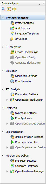
The Flow Navigator is the most important pane of the main Vivado window to know. It is how a user navigates between different tools within Vivado.
The Navigator is broken into seven sections:
- Project Manager
- Access project settings, add new source files, view snippets of useful RTL code, and add components of a hardware design (IP) included within the tool to your own design.
- IP Integrator
- Create a hardware design through the use of a Block Design by connecting IP blocks together.
- Simulation
- Debug and verify a hardware design fully within software, without deploying it to hardware.
- RTL Analysis
- See how the tools are interpreting a design by viewing the circuit that the design describes.
- Synthesis
- Modify Synthesis settings and view post-synthesis reports - determine whether the design meets timing, and how much of the chip resources it will use.
- Implementation
- Modify Implementation settings and view post-implementation reports - determine whether the design meets timing, and how much of the chip resources it will use.
- Program and Debug
- Access to settings for bitstream generation and the Hardware Manager. Used to build a design and deploy it to a board.
The Project Manager
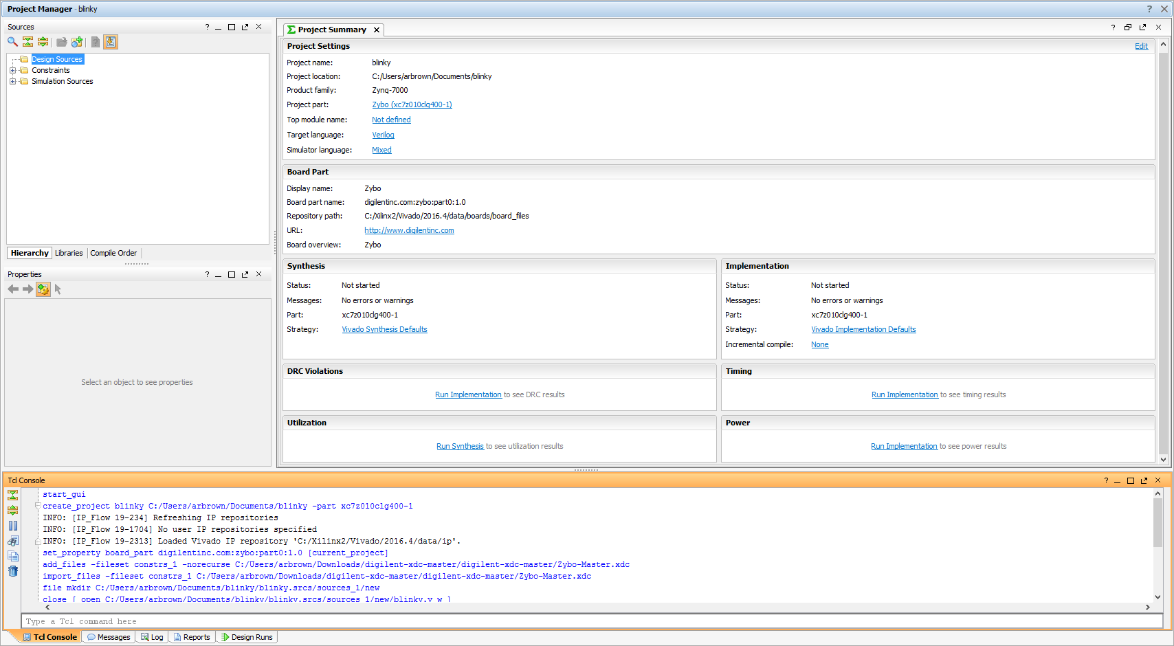
This tool is where most development will occur and is the initial tool open after creating a new project.
The Project Manager consists of four panes, Sources, Properties, Results, and the Workspace.
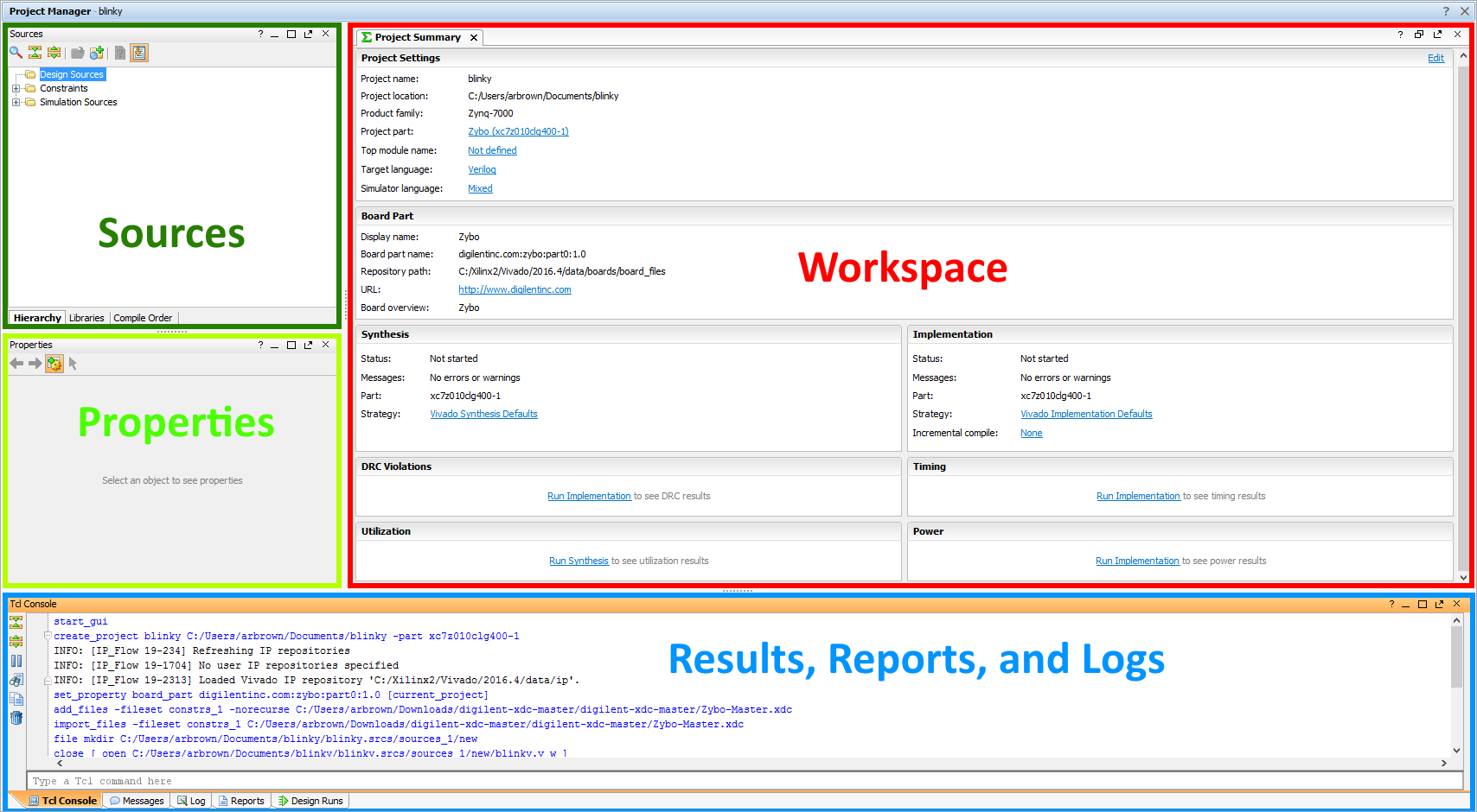
The Sources pane contains the project hierarchy and is used for opening up files. The folder structure is organized such that the HDL files are kept under the Design Sources folder, constraints are kept under the Constraints folder, and simulation files are kept under the Simulation Sources folder. Files can be opened in the Workspace by double-clicking on the corresponding entry in the Sources pane. Sources can also be added by either right-clicking the folder to add the file to and selecting Add Sources or by clicking the Add Sources button ( ).
).

The Properties pane allows for viewing and editing of file properties. When a file is selected in the Sources pane its properties are shown in here. This pane can usually be ignored.

The unnamed pane at the bottom of the Project Manager window consists of several different useful tools for debugging a project. The most important one to know is the Messages tool. This tool parses the Tcl console for errors, warnings, and other important information and displays it in an informative way.
These tools can be accessed by selecting the different tabs at the bottom of this pane.
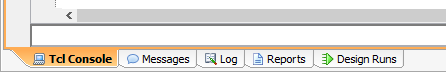
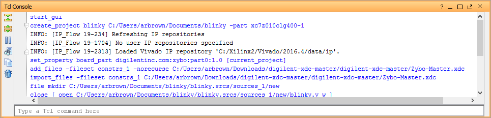
The Tcl Console is a tool that allows for running commands directly without the use of the main user interface. Some messages may link to the Tcl Console to provide more information regarding an error.
The Reports tool is useful for quickly jumping to any one of the many reports that Vivado generates on a design. These reports include power, timing, and utilization just to name a few.

The Log displays the output from the latest Synthesis, Implementation, and Simulation runs. Digging into this is usually not necessary as the reports and messages views store the information in the log in a more readable format.

The last tool is the Design Runs. Using this tool run settings can be edited and new runs can be created. This tool is useful when targeting multiple devices with the same design.

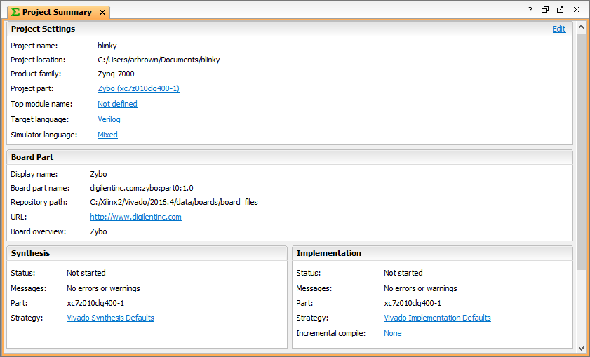
The most important pane in the Project Manager is the Workspace. The Workspace is where reports are opened for viewing and HDL/constraints files are opened for editing. Initially, the Workspace displays the Project Summary which show some basic information from some of the reports.
Adding a Constraint File
Constraint files describe the requirements put upon a design by the components surrounding an FPGA - including all peripherals, external clocks, and more.
In order to connect the ports found in an RTL top module (described later) with the physical pins of the FPGA, a constraint file needs to be added or created. Digilent provides Xilinx Design Constraint (XDC) files for each board. Download digilent-xdc-master.zip, the ZIP Archive containing each of these master XDC files, then extract it in a location you will remember.
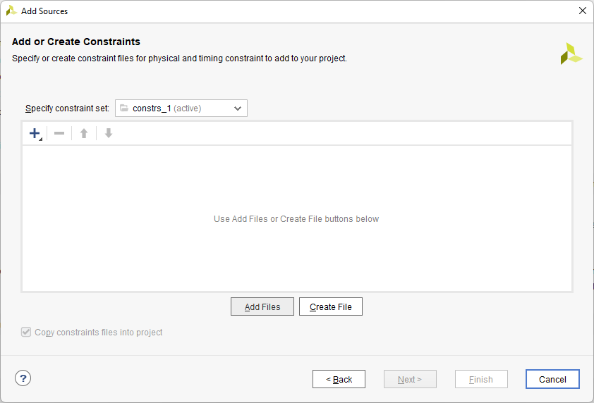
In the Project Manager section of the Flow Navigator, click the  button. In the wizard that pops up, select Add or create constraints then click Next.

At this stage, Vivado provides a list of all of the constraint files that will be added or created when we click Finish. Currently, this list is empty, this will change when files have been added or created. A constraint file will not be created from scratch in this guide, so click Add Files.
Find the directory you extracted the digilent-xdc-master.zip archive into, then click on the file for your board. This should add the name of the file to the File Name field.
Click OK to continue.

Make sure that the selected XDC file has been added to the list of sources, and that the Copy constraint files into project is checked, then click Finish.
Note: Leaving the Copy… box unchecked means that any editing done to the constraint file will be reflected in the original copy. Checking the box is highly recommended

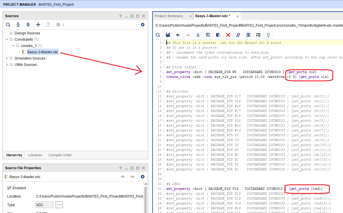
Find the (.xdc) constraints file in the Sources section of the project. Double-click it to view the contents. This is the file that maps your design signal names to FPGA pins. In this example, we are going to use clk for the system clock and led for the indicator led[0]. There are three lines of interest, two for the system clock and one for a led[0]. For the BASYS3, these lines happen to be 7 & 8 and 31, shown in the image to the right. Uncomment these by removing the leading # character and make sure the get_ports name is [get_ports clk] for the clock and [get_ports led] for led[0]. If you have a different board, do the same but the line numbers may be different. Our Verilog design module will use clk and led for input and output. The last step is to save the constraint file changes by clicking the save icon.
1. On some boards, the clock port will consist of two different ports, clk_p and clk_n. On others, it may be named something like sysclk, but always appears at the top of the XDC file.
2. A board using clk_p and clk_n pins means that the input clock uses differential logic. If you want to know more, read this article on low-voltage differential signaling.
Creating a Verilog Source File
Verilog is one of several hardware description languages (HDLs) that can be used within Vivado to describe a circuit to be implemented within an FPGA. This section describes how to create a Verilog file within Vivado, and create a simple circuit that will work on any Digilent FPGA development board.
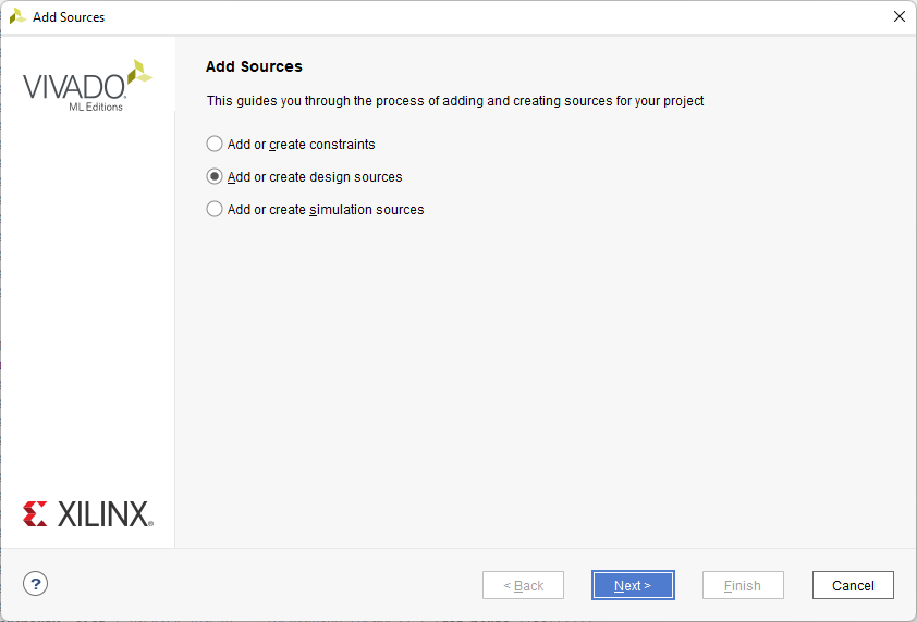
In the Project Manager section of the Flow Navigator, click the button again. Select Add or create design sources then click Next.
As before, at this stage, we will be provided a list of all of the source files that will be added or created when we click Finish. Instead of clicking Add Files, click Create File.
Note: It is also possible to add existing source files in the same way the constraint file was added, above.

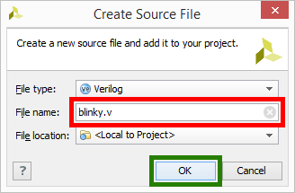
You will be prompted to select a File type, File name, and File location. Make sure to pick Verilog and <Local to project> for the type and location. Give your file a name ending in '.v'.
Important: Do NOT use spaces in your file name. This will cause problems with Vivado. Instead use an underscore, a dash, or CamelCase.
Click OK to continue.
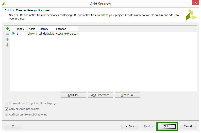
Make sure that the new Verilog source file has been added to the list of sources, then click Finish.
Unlike when the constraint file was added, at this point, a Define Module dialog will pop up. You can rename your Verilog module using the Module name field, but this is unnecessary. The Verilog module's clock and led ports need to be defined. Clicking the Add ( ) button will add an empty slot for a port to the I/O Port Definitions list.
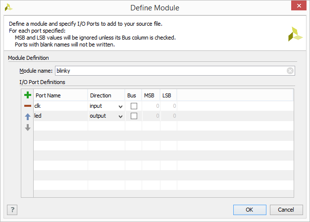
There are five fields to define for each of the module's I/O ports:
- Port Name: This field defines the name of the port and needs to match one of the names you used in your XDC file.
- Direction: This drop-down menu can be set to input, output, or inout, defining the direction that signals propagate through this port, with respect to your module. Outputs are the signals that your module will be controlling.
- Bus: This can be checked or not, when checked, this port consists of multiple single-bit signals, grouped into a single bus.
- MSB: The index of the most significant bit of the port, if it is a bus. This option is grayed out for single-bit ports.
- LSB: The index of the least significant bit of the port, if it is a bus. This option is grayed out for single-bit ports.
Note: If you are defining a module that will be instantiated in another module, which we will not go into in this guide, be aware that the port names of non-“top” modules should not be declared in the XDC.
If your board uses differential clocking, add two single-bit input ports with the same names as the positive and negative clock ports that were uncommented in your XDC file. Otherwise, add a single single-bit input port with the same name as the clock port that was uncommented in your XDC file.
Add a single-bit output port with the same name as the LED port that was uncommented in your XDC file.
Once these two or three ports have been added, click OK to continue.
At this point, the new source file will be added to the Design Sources folder in the Sources pane of the Project Manager. Expand this folder and double-click on the file to open it.
Next, some Verilog code needs to be written to define how the design will actually behave.

Between the ');' that comes after the module's port list and the 'endmodule' statement, add the following lines of code.
This snippet of code implements a 25-bit counter, which will increment by 1 every clock cycle, and roll back over to 0 after ~33 million cycles (about a third of a second, given a 100MHz input clock). The LED is directly driven by the top bit of the counter, which, of the bits, changes the least frequently. Given a 100MHz clock, the LED will blink (go through a full cycle of low-to-high-to-low transitions) approximately three times per second.
reg [24:0] count = 0;

assign led = count[24];

always @ (posedge(clk)) count <= count + 1;
If your board is differentially clocked, add the following lines of code after ');' and before the 'reg [24:0] count = 0;' line.
This instantiates a differential input buffer, which will allow you to get a non-differential clock that can be used to clock the FPGA fabric.
wire clk;

IBUFGDS clk_inst (
    .O(clk),
    .I(clk_p),
    .IB(clk_n)
);
It should be noted that the rate at which the clock will blink will differ depending on the board used. System clocks on different Digilent boards run at a number of different rates, depending on the needs of the board. The system clock period in nanoseconds can be found on the create_clock line of the XDC file.
After completing this guide, it is suggested to try changing the provided Verilog code so that the clock blinks at 1 Hertz. (Note that the XDC file only describes the period of the input clock, and changing it will only misinform the tools, rather than changing the input clock period)
Generate a Bitstream
In order to create a file that can be used to program the target board, each stage of the “compilation pipeline” needs to be run.
This starts with Synthesis. Synthesis creates a description of the logic gates and connections between them required to perform the functionality described by the HDL files, given the constraints included in XDC files. To run Synthesis click either  in the toolbar or
 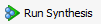 in the Flow Navigator. The output of Synthesis is then passed to Implementation.
Implementation has several steps. The steps that are always run are Opt Design (Optimize the design to fit on the target FPGA), Place Design (Lay out the design in the target FPGA fabric), and Route Design (Route signals through the fabric). To run Implementation click either  in the toolbar or
 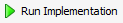 in the Flow Navigator. This output is then passed on to the Bitstream Generator.
The Bitstream Generator generates the final output file needed for programming the FPGA. To run Bitstream Generation click either  in the toolbar or
 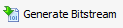 in the Flow Navigator. With no settings changed, the generator will create a '.bit' file.
Depending on the complexity of the design, the board used, and the strength of your computer, the process of building the project can take between 5 and 60 minutes. When complete, a pop-up dialog will appear, prompting you to select one of several options. None are relevant for the purposes of this guide, so click Cancel. The “write_bitstream complete” status message can be seen in the top right corner of the window, indicating that the demo is ready to be deployed to your board.
Programming an FPGA Board through Vivado's Hardware Manager
Vivado's Hardware Manager can be opened by clicking on Open Hardware Manager at the bottom of the Flow Navigator pane on the left side of the Vivado window.

The first step to programming a device is to connect the Vivado Hardware Server to it as a target. To get to the Open Hardware Target wizard click the  link in the green banner near the top of the window. From the drop-down that opens, select
  .
.
Once the wizard opens, click Next.

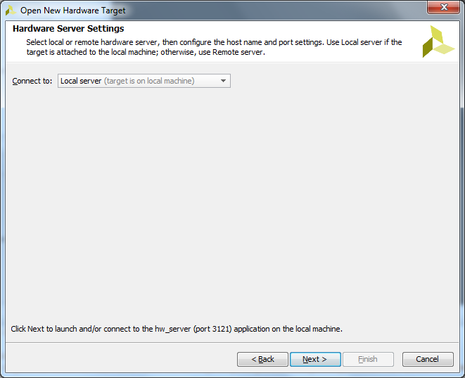
The next screen asks if the hardware server is local or remote. If the board is connected to the host computer choose local, if it is connected to another machine choose remote and fill in the Host Name and Port fields.
Click Next to continue.
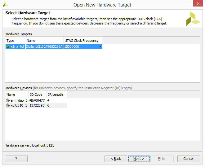
This screen gives a list of devices connected to the hardware server. If there is only one connected it will be the only device shown.
Click Next to continue.
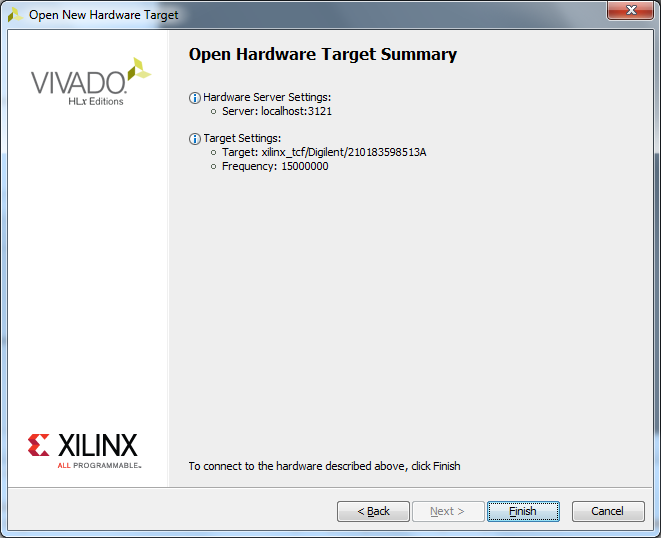
The final screen shows a summary of the options selected in the wizard. Verify the information and click Finish. The board is now connected to the hardware server.
To program the device with the bit file generated earlier, either click the  link in the green banner at the top of the window or click the
  button in the Flow Navigator under
  . From the drop-down that opens, select the device to program (Example:
  ) and the following window will open:
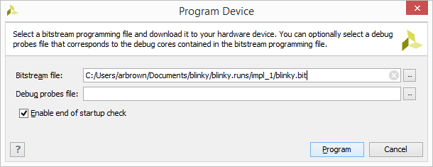
The Bitstream File field should be automatically filled in with the bit file generated earlier. If not, click the  button at the right end of the field and navigate to
<Project Directory>/<Project Name>.runs/impl_1/ and select the bit file (Example:  ). Now click Program. This will connect to the board, clear the current configuration, and program it using the new bit file.
In Conclusion
You should now see one of the LEDs on your board blinking!
Be sure to visit your board's resource center for more tutorials and demo projects. A link to each resource center can be found on this wiki's Programmable Logic page.