Real Analog: Chapter 5
- Chapter 5 Materials
-
- Lecture Material:
- Lecture 12b PowerPoint Slides: Derivation of maximum power transfer, Thévenin theorem examples, operational amplifiers
- Lecture 13 PowerPoint Slides: Operational amplifier examples, dependent Sources
- Chapter 5 Video:
- Lab 5 Video: Operational amplifiers: Constructing operational amplifier based circuits.
-
-
- Exercise Solutions: Chapter 5 exercise solutions
- Homework: Chapter 5 homework problems
5. Introduction and Chapter Objectives
Operational amplifiers (commonly abbreviated as op-amps) are extremely useful electronic devices. Some argue, in fact, that operational amplifiers are the single most useful integrated circuit in analog circuit design. Operational amplifier-based circuits are commonly used for signal conditioning, performing mathematical operations, and buffering. These topics are discussed briefly below.
Signal conditioning is the process of manipulating a given signal (such as a voltage) to improve its properties or usefulness. Examples of common signal conditioning processes are:
- Level adjustment: the overall level of a signal may be too small to be usable. For example, the voltage output from a thermocouple (an electrical component used to measure temperature) may be only a few thousandths of a volt. It is often desirable to amplify the signal to increase the output voltage – this is often done using circuits containing operational amplifiers.
- Noise reduction: electrical signals are susceptible to noise; an undesirable component of a signal. (For example, static on a radio signal.) Operational amplifier circuits can be used to remove, or filter out undesirable components of a voltage signal.
- Signal manipulation: Electrical signals are often used to transmit information. For example, the voltage output of a thermocouple changes as the temperature of the thermocouple changes. The sensitivity of the thermocouple output to temperature changes may be changed by an operational amplifier circuit to provide a more readily usable output voltage-to-temperature relationship.
A common use of electrical circuits is to perform mathematical operations. So far, we have focused on developing mathematical models of existing circuits – we have been performing analysis tasks. The design process, conversely, can be considered to consist of implementing an electrical circuit that will perform a desired mathematical operation. (Of course, a large part of the design process consists of determining what mathematical operation is to be performed by the circuit.) Operational amplifier circuits are readily developed to perform a wide range of mathematical operations, including addition, subtraction, multiplication, differentiation, and integration.
Buffers allow us to electrically isolate one section of an electrical circuit from another. For example, using an electrical circuit to supply power to a second electrical circuit may result in undesirable loading effects, in which the power requirements of the second circuit exceed the power that the first circuit can provide. In this case, a buffer can be used to isolate the two circuits and thus simplifying design problems associated with integrating the two circuits. Operational amplifier circuits are commonly used for this purpose.
Operational amplifiers (or op-amps) are active devices. This differs from passive devices, such as resistors, in that an external power source must be provided to the operational amplifier in order to make it function properly. Op-amps are rather complex devices, consisting of a number of interconnected transistors and resistors. We will not be interested at this point in a detailed description of the internal operation of operational amplifiers – instead, we will use an op-amp model which provides us with relatively simple input-output relations for the overall circuit. In fact, our op-amp model will most often take the form of a dependent source1). In their most basic form, operational amplifiers are most readily modeled as voltage controlled voltage sources, but it can be used within other circuits to create devices which act as other types of dependent sources. This simplified model will be adequate for many analysis and design purposes.
The operational amplifier symbol which we will most often use is shown in Figure 5.1. Operational amplifiers are essentially three-terminal devices (ignoring the power supply connections previously mentioned for the moment), having two input terminals and one output terminal. The inputs are called the inverting terminal (indicated by the – sign) and the non-inverting terminal (indicated by the + sign). We will use $v_n$ and $i_n$ to denote the voltage and current at the inverting terminal, and $v_p$ and $i_p$ to denote the voltage and current at the non-inverting terminal. The voltage and current at the output terminal are denoted as $v_{OUT}$ and $i_{OUT}$.The voltages $v_p$, $v_n$, and $v_{OUT}$ are all measured relative to some common reference voltage level, such as ground.
After Completing this Chapter, You Should be Able to:
- State ideal operational amplifier modeling rules
- State constraints on the operational amplifier output voltage
- Represent operational amplifiers as dependent voltage sources
- Be able to identify standard operational amplifier pin connections
- Analyze electrical circuits containing ideal operational amplifiers and resistors
- Sketch op-amp based circuits which perform the following operations:
- Inverting voltage amplification
- Non-inverting voltage amplification
- Summation (addition)
- Differencing (subtraction)
- Buffering
- Describe the operation of a comparator
- Briefly describe the effect of the following non-ideal op-amp parameters, relative to ideal op-amp performance:
- Finite input resistance
- Finite output resistance
- Finite op-amp gain
5.1: Ideal Operational Amplifier Model
We will begin by summarizing the rules governing ideal operational amplifiers. In the following section, we will provide some background material relative to these rules and some additional criteria which the operational amplifier must satisfy. It should be emphasized that these rules govern ideal operational amplifiers; modeling of non-ideal operational amplifiers will most likely be presented in later electronics courses.
Ideal Op-amp Modeling Rules
- No current flows into the input terminals: $i_n = i_p = 0$
- The voltages at the input terminals are the same: $v_n = v_p$ (when sufficient negative feedback is applied).
No requirements are placed on the output voltage and current. One may not conclude that $i_{OUT} = 0$ simply because the input currents are zero. It may appear, from the input-output relations governing the op-amp, that the op-amp violates Kirchhoff’s current law – this is because we are not examining the details of the internal operation of the op-amp. Since the op-amp is an active device with its own power supply, it can provide an output current with no input current. Operational amplifiers, unlike passive devices, are capable of adding power to a signal. The presence of the external power supplies raises some additional constraints relative to op-amp operation; we address these issues next.
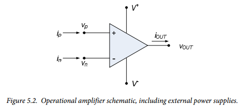
A more complete schematic symbol for an operational amplifier, including the op-amp’s external power supplies, is shown in Figure 5.2. Figure 5.2 shows two additional op-amp terminals. One is connected to a voltage source $V^+$ and the other is connected to a voltage source $V^-$. These terminals are sometimes called the positive and negative power supply terminals. We must set the external voltage supplies so that the positive power supply voltage is greater than the negative power supply voltage: $V^+ > V^-$. In our discussions, it will be assumed that the power supply voltages are relative to the same reference voltage as all other voltages on the schematic.
The power supply voltages provide a constraint on the range of allowable output voltages, as provided below:
Output Voltage Constraint:
- The output voltage is constrained to be between the positive and negative power supply voltages: $V^- < v_{OUT} < V^+$.
The above constraint is based on pure inequalities – in general, the output voltage range will be somewhat less than the range specified by V- and V+. The margin between the output and the supply voltages will vary depending on the specific op-amp. Any attempt to drive the output voltage beyond the range specified by the supply voltages will cause the output to saturate at the appropriate supply voltage. Similarly it makes sense that the power supply voltages will constrain the range of allowable input voltages, as provided below:
Input Voltage Constraint:
- The input voltages, $v_p$ and $v_n$, are constrained to be between the positive and negative power supply voltages: $V^- < v_p, v_n < V^+$.
The above constraint is based on pure inequalities – in general, the input voltage range will be somewhat less than the range specified by V- and V+. The margin between the inputs and the supply voltages will vary depending on the specific op-amp. Any attempt to drive the input voltages beyond the range specified by the supply voltages will cause the op-amp to no longer operate as we describe in this simple ideal model.
It is important to keep in mind, when analyzing operational amplifier circuits, that all of the terminal voltages shown in Figure 5.2 should be taken as having the same reference voltage2). Figure 5.3 provides an explicit illustration of what is implied by this statement.
All voltages in Figure 5.3, including the power supply voltages $V^+$ and $V^-$, have the same reference. It is obvious from Figure 5.3 that KCL at the reference node provides:
$$i_p + i_n = i_- + i_{OUT} + i_+ = 0$$
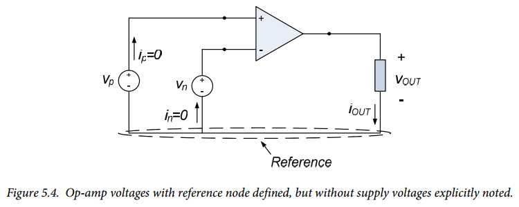
So that the positive and negative power supplies provide the current to the output. However, it is common to leave the power supply terminals off of the op-amp diagram (as in Figure 5.1). If one interprets these types of diagrams literally, the figure corresponding to Figure 5.3 will be as shown in Figure 5.4.
Now, if one attempts to blindly apply KCL at the reference node of Figure 5.4, one obtains:
$$i_p + i_n = i_{OUT} = 0$$
And it is tempting to infer that the current out of the op-amp must be zero. This is not true; it is a misconception based upon an attempt to literally interpret a somewhat incomplete schematic.
Section Summary
- The operational amplifier symbol is:
- The operation of ideal operational amplifiers follows the rules below:
- No current flows into the input terminals: $i_n = i_p = 0$
- The voltages at the input terminals are the same: $v_n = v_p$
- The output voltage is constrained to be between the positive and negative power supply voltages: $V^- < v_{OUT} < V^+$
- Nothing is known about the current out of the op-amp, $i_{OUT}$
- All voltages on the above diagram are relative to the same reference.
Exercises
- The op-amp in the circuit with negative feedback below is ideal. Find:
- The current $I_s$
- The voltage $V_p$
- The voltage $V_n$
5.2: Operational Amplifier Model Background
The rules provided in section 5.1 governing our ideal operational amplifier model can be applied directly to operational amplifier circuits, but some background information will allow more insight into the basis for these rules. We will still treat the operational amplifier as a single circuit element with some input-output relationship, but our more complete description will model the op-amp as a dependent source. Certain assumptions relative to this dependent source allow us to recover the op-amp rules presented in section 5.2, but our more complete model will allow us to later introduce some basic non-ideal operational amplifier effects.
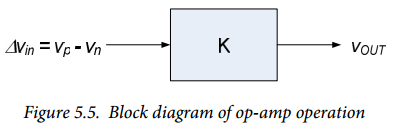
An operational amplifier operates as a differential amplifier with a very high gain. That is, the output of the amplifier is the difference between the input voltages, multiplied by a large gain factor, K. Figure 5.5 shows the operation of the op-amp, from a systems-level standpoint:
Thus, the input-output relation for an operational amplifier is:
$$V_{OUT} = K \left(v_p - v_n \right) = K \cdot \Delta v_{in} (Eq. 5.1)$$
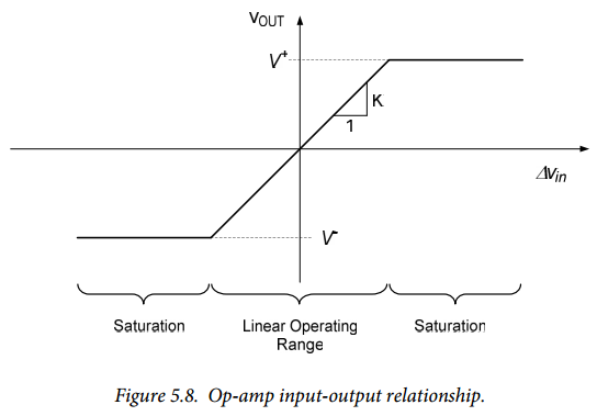
Where in $\Delta v_{in}$ is the difference between the voltages at the input terminals and K is a very large number. (Values of K for typical commercially available operational amplifiers can be on the order of $10^6$ or higher.) Since the output voltage is constrained to be less than the supply voltages,
$$V^- < K \cdot \Delta v_{in} < V^+$$
So
$$\frac{V^-}{K} < \Delta v_{in} < \frac{V^+}{K} (Eq. 5.2)$$
If the voltage supplies are finite and K is very large, the difference in the input voltages must be very small. Thus,
$$\Delta v_{in} \approx 0$$
And $v_p \approx v_n$. This is of course only true when $V^- < v_{OUT} < V^+$.
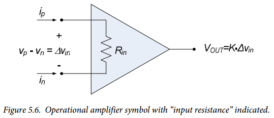
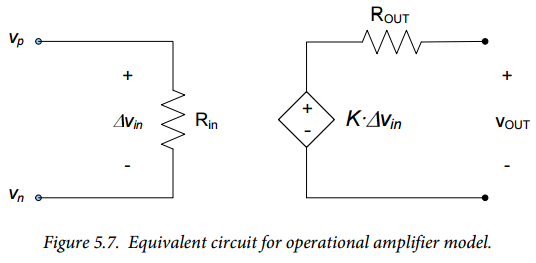
The second operational amplifier modeling rule is a result of the high input resistance of operational amplifiers. We assume that any difference in the input terminal voltages is due to the operational amplifier’s input resistance, $R_{in}$, times the current at the input terminals. This is illustrated conceptually in Figure 5.6.
From Figure 5.6, we see that the voltage difference between the input terminals can be considered to result from an input current passing through this input resistance.
$$v_p - v_n = R_{in} \cdot i_p$$
We will also assume that KCL applies across the input terminals of Figure 5.6, so that:
$$i_p = - i_n$$
The above equations can be combined to give:
$$i_p = - i_n = \frac{v_p - v_n}{R_{in}} (Eq. 5.3)$$
Since the input resistance of operational amplifiers is very large (commercial operational amplifiers have input resistances of several mega-ohms or higher) and the voltage difference across the input terminals is very small,
$$i_p = - i_n \approx 0 $$.
The above results suggest that an operational amplifier operates as a voltage-controlled-voltage source as shown in Figure 5.7. Typically, commercially available operational amplifiers have very high gains, K, very high input resistances, $R_{in}$, and very low output resistances, $R_{out}$.
Combining the criteria provided by equations (5.1) and (5.2) results in the input-output relationship shown graphically in Figure 5.8 below. The circuit operates linearly only when the output is between the supply voltages. When the output attempts to go outside this range, the circuit saturates and the output remains at the appropriate supply voltage. Notice that the negative supply voltage in Figure 5.8 is indicated as a negative number; this is fairly typical, though not a requirement.
Our ideal operational amplifier model rules are based on the above, more general, operational amplifier relationships. The assumptions relative to ideal operational amplifier operation, along with their associated conclusions, are provided below:
- The output voltage is bounded by the power supply voltages: $V^- < v_{OUT} < V^+$
- $K \rightarrow \infty$. This, in conjunction with equation (5.2) implies that $\Delta v_{in} = 0$ and $v_p = v_n$.
- $R_{in} \rightarrow \infty$. This, in conjunction with equation (5.3) implies that $i_p = - i_n = 0$.
- $R_{OUT} = 0$.
Section Summary
- A circuit modeling the behavior of an operational amplifier is:
- For ideal operational amplifiers, the parameters in the circuit above are:
- $K \rightarrow \infty$. This implies that $\Delta v_{in} = 0$ and $v_p = v_n$.
- $R_{in} \rightarrow \infty$. This implies that $i_p = - i_n = 0$.
- $R_{OUT} = 0$. This implies that the operational amplifier can provide infinite power as its output.
- In the operational amplifier model above, it is still assumed that $V^- < v_{OUT} < V^+$.
Exercises
- An operational amplifier has a gain K = 10,000. The voltage supplies are $V+ = 20V$ and $V-= -10V$. Determine the output voltage if the voltage difference between the input terminals $\left( v_p - v_n \right)$ is:
- 1mV
- 2mV
- 4mV
- -0.2mV
- -2mV
5.3: Commercially Available Operational Amplifiers
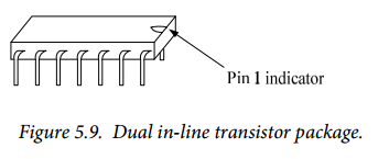
Operational amplifiers are available commercially as integrated circuits (ICs). They are generally implemented as dual in-line packages (DIPs), so called because the terminals (pins) on the package are in pairs and line-up with one another. A typical DIP is shown in Figure 5.9. The pins on DIPs are numbered; in order to correctly connect the DIP, pin 1 must be correctly oriented. Pin 1 is commonly located by looking for a notch at one end of the IC – pin 1 will be to the immediate left of this notch, if you are looking at the IC from the top. Alternate methods of indicating pin 1 are also used: sometimes the corner of the IC nearest pin 1 is shaved off or a small indentation or dot is located at the corner of the IC nearest pin 1.
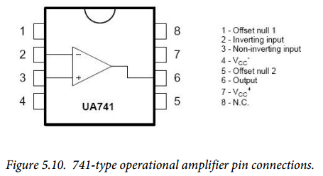
One common op-amp device is the 741 op-amp. The 741 is an eight-lead DIP; a top view of the package, with the leads labeled, is shown in Figure 5.10. Key features of the package are as follows:
- Orientation of the pins is determined by the location of a semicircular notch on the package, as shown in Figure 5.10. (Recall that Figure 5.10 is a top view of the device.) Alternately, some packages place a circular indentation near pin 1 in order to provide the orientation of the pins.
- Inverting and non-inverting inputs are pins 2 and 3, respectively in Figure 5.10
- The output terminal is pin 6 on the package.
- The positive and negative power supplies are labeled as $V_{CC}+$ and $V_{CC}-$ in Figure 5.10. They are pins 7 and 4, respectively. $V_{CC}+$ should be less than +15 volts and $V_{CC}-$ should be more than -15 volts. A larger range of power supply voltages may destroy the device.
- The pins labeled OFFSET NULL 1, OFFSET NULL 2, and NC (pins 1, 5, and 8) will not be used for this class. The offset null pins are used to improve the op-amp’s performance. The NC pin is never used. (NC stands for “not connected”).
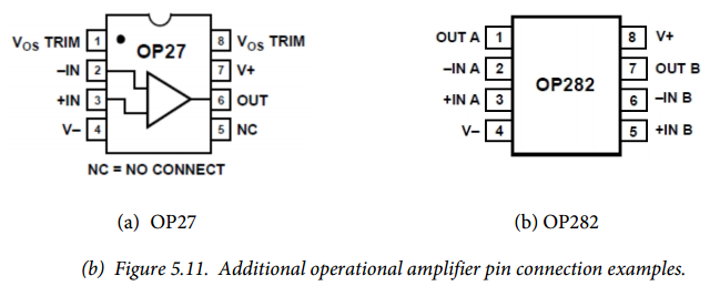
Most commercially available operational amplifiers will conform to a relatively standard pin connection layout. However, there will tend to be variations to one extent or another. For example, pin connections for an OP27 operational amplifier are shown in Figure 5.11(a). Some operational amplifier chips will also contain more than one operational amplifier on the chip. For example, Figure 5.11(b) provides pin connections for an OP282 package, in which two operational amplifiers are included. (A chip with two operational amplifiers is commonly called a “dual package”. Chips with four operational amplifiers are also common; they are often called “quad packages”.) In Figures 5.11, V+ and V- are the positive and negative power supplies, respectively. (Both operational amplifiers on the OP282 chip share the same power supplies.) +IN and –IN are the positive and negative input terminals, and OUT is the output terminal. In the OP27 amplifier, the VOS TRIM terminals perform the same purpose as the Offset Null pins on the 741-type operational amplifier. The OP282 chip contains two amplifiers, “A” and “B”. In Figure 5.11(b), the inputs and outputs for the two amplifiers are identified as being associated with the “A” or “B” amplifier by appending the appropriate letter.
Note
Always check the manufacturer’s data sheet for the specific operational amplifier you are using. This can eliminate irritating and time-consuming errors when wiring your circuits!
Exercises
- Go to the Analog Devices website, and look up the pin connections for the OP482 operational amplifier package. Sketch the package and label the pin connections. Briefly describe your interpretation of the various pin connections.
5.4: Analysis of Op-amp Circuits
Operational amplifiers can be used as either linear or nonlinear circuit elements. When used as nonlinear circuit elements, the op-amp is deliberately operated so that the output voltage from the op-amp is driven to the power supply voltages. In this mode of operation, the output of the op-amp is said to be saturated and does not necessarily change as the input to the system changes. When the operational amplifier is used as a linear circuit element, the output is maintained within the range of the power supply voltages and the output voltage is a linear function of some input voltage or voltages.
In this chapter, we will be concerned with the use of operational amplifiers as linear circuit elements. When used in this mode, the overall circuit is generally constructed to provide negative feedback around the operational amplifier itself. When operated in a negative feedback mode, the output of the operational amplifier is connected to the inverting input terminal, generally through some other circuit elements. Negative feedback tends to make the overall circuit less sensitive to the specific value of the op-amp gain and reduces the likelihood of saturation at the op-amp output. We will not be concerned here with the details of why this is true, beyond noting that these devices will generally not operate linearly without feedback. (Later electronics courses will discuss why this is true.)
Nodal analysis is often the most efficient way to approach the analysis of an operational amplifier-based circuit. When applying nodal analysis to a circuit containing an ideal operational amplifier, the first step should be to apply the basic op-amp rules to the overall circuit. These were presented in the previous chapter, and are repeated here for convenience:
- The voltages at the input terminals of the operational amplifier are the same.
- The currents into the input terminals of the operational amplifier are zero.
It should be emphasized that application of rule 1 above does not imply that both of the op-amp input terminals can be treated as being part of the same node. The op-amp input terminals should be treated as being two separate nodes, with the same voltage potential. After applying the basic op-amp rules, it is generally appropriate to apply Kirchhoff’s current law at the input terminals of the operational amplifier. Additional nodes in the circuit may necessitate application of KCL at other points, but the above approach is generally an extremely good starting point.
Important Tip:
Applying KCL at the output node of an operational amplifier is often not productive. Since no information is available about the current out of an operational amplifier (due to the active nature of the device, as noted in the previous section) application of KCL at the output node generally provides an additional equation, at the expense of introducing an additional unknown. Application of KCL at an op-amp output node is generally only productive if one must determine the current output of the op-amp.
When analyzing an operational amplifier as a linear circuit element, the external power supply voltages will generally be ignored. We will assume that the output voltage is within the voltage range specified by the external power supplies. If the output voltage is not within this range, the circuit will not behave linearly, and our analysis will be invalid. The final step of any analysis of an operational amplifier circuit is to determine whether the output voltage is within the external power supply voltage range; meeting this constraint often results on a constraint on the input voltages applied to the circuit.
Suggested Analysis Approach:
- Apply ideal operational amplifier rules to circuit. (Voltage potentials at op-amp input terminals are the same; no current enters the op-amp input terminals.)
- Apply KCL at op-amp input terminals.
- Apply KCL at other circuit nodes, if necessary.
- Check to ensure that output voltage remains within range specified by op-amp power supply voltages.
We illustrate the above analysis approach with several examples. The example circuits provided below illustrate the use of operational amplifier circuits to perform the mathematical operations of scaling (multiplication by a constant), addition, and subtraction. We also provide an example circuit which performs a buffering operation – this circuit can be useful for isolating different parts of a circuit from one another.
Example 5.1
Determine $V_{OUT}$ as a function of $V_{IN}$ for the circuit shown below.
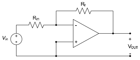
Choosing the non-inverting terminal voltage as our reference voltage and applying the ideal operational amplifier rules allows us to label the voltages and currents shown in red below.
Applying KCL at the non-inverting input terminal provides no information (we know the current and voltage at the non-inverting input). Applying KCL at the inverting input terminal results in:
$$i_{in} = i_f$$
Using Ohm’s law to write these currents in terms of node voltages and taking advantage of the fact that the voltage at the inverting terminal of the op-amp is zero (because there is no voltage difference across the input terminals of the op-amp and we have chosen the non-inverting terminal voltage as our reference) results in:
$$\frac{V_{in} - 0}{R_{in}} = \frac{0 - V_{OUT}}{R_f}$$
Solving the above for $V_{OUT}$ results in:
$$V_{OUT} = - \left( \frac{R_f}{R_{in}} \right) V_{in}$$
Comments:
- This circuit is called an inverting voltage amplifier. The output voltage is a scaled version of the input voltage, hence the term “voltage amplifier”. The change in sign between the output and input voltage makes the amplifier “invert”.
- The output voltage must be between the op-amp power supply voltages. Depending on the values of $R_f$ and $R_{in}$, this sets limits on the magnitude of the input voltage to avoid saturation.
It is worthwhile at this point to make a few comments relative to some concepts presented sections 5.1 and 5.2, in the context of the op-amp circuit of Example 5.1.
- The input-output relationship governing the circuit of Example 5.1 can be represented conceptually as a dependent source-based circuit. The input-output relationship for the circuit, as determined in Example 5.1, is:
$$V_{OUT} = - \left( \frac{R_f}{R_{in}} \right) V_{in}$$
While the current provided by the source to the circuit is:
$$i_{in} = \frac{V_{in} - 0}{R_{in}}$$
These two relationships are satisfied by the voltage controlled voltage source (VCVS) shown in Figure 5.12 below. The input resistance of this circuit is the resistance $R_{in}$; the input resistance governs the relationship between the voltage applied by the source and the source current necessary to maintain that voltage. Thus, increasing $R_{in}$ reduces the power which the source must provide to maintain the output voltage $V_{out}$.
Note:
The input resistance of the circuit of Example 5.1 is not the same as the input resistance of the operational amplifier itself, as shown in Figures 5.6 and 5.7.
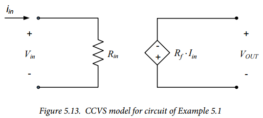
- The representation given in Figure 5.12 of the circuit of Example 5.1 is not unique. For example, the current controlled voltage source (CCVS) model shown in Figure 5.13 is also a valid model for the circuit.
- The circuit of Example 5.1 has an open-circuit at the op-amp output terminal. Thus, no current is provided to the output. However, this does not imply that the current at the output terminal of the op- amp is zero! KCL at the op-amp output terminal indicates that the current through the feedback resistor goes into the op-amp output terminal, where (from our diagram) it seems to disappear! Recall, however, from our discussion in section 5.1 (see, in particular, Figure 5.3) that this current will pass through the supply voltages and then to the reference node. The supply voltages and their associated path to the reference node are not shown on the circuit diagram in Example 5.1, but they do exist.
- If we apply a load resistor $R_L$ to the output terminal of the operational amplifier in Exercise 5.1, we obtain the circuit shown in Figure 5.14. The analysis of the circuit proceeds exactly as in Exercise 5.1, and we again obtain:
$$V_{OUT} = - \left( \frac{R_f}{R_{in}} \right) V_{in}$$
This result does not depend on the current through the load, $i_L$! This is because we made no assumptions relative to the current out of the operational amplifier output; the operational amplifier adjusts its output current as necessary to provide the current required to maintain the output voltage as in the above expression.
Note:
Our ideal operational amplifier will draw power from the supply voltages to provide whatever output current is necessary to satisfy the rules governing operational amplifier provided in section 5.1. Real operational amplifiers, of course, have current limitations. We will discuss these limitations in section 5.6.
Example 5.2
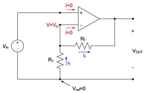
Determine $V_{OUT}$ as a function of $V_{IN}$ for the circuit shown below.

Choosing our reference voltage at the negative terminal of both $V_{in}$ and $V_{OUT}$ and applying the ideal operational amplifier rules allows us to label the voltages and currents shown in red below. (Note that since the input voltage sets the voltage of the non-inverting op-amp terminal, it also indirectly sets the voltage at the inverting terminal of the op-amp.)
Applying KCL at the inverting terminal of the op-amp results in $i_1 = i_f$. Using Ohm’s law to write these in terms of voltages provides:
$$\frac{0-V_{in}}{R_1} = \frac{V_{in} - V_{OUT}}{R_f}$$
Solving this for $V_{OUT}$ gives $V_{OUT} = \left( 1 + \frac{R_f}{R_{in}} \right) V_{in}$
Comments:
- The output voltage can be expressed as a gain (a multiplicative factor) times the input voltage; the circuit is a “voltage amplifier”. Since there is no sign change between the input and output voltage, the circuit is a non-inverting voltage amplifier.
- The output voltage must be between the op-amp power supply voltages. Depending on the values of $R_f$ and $R_1$, this sets limits on the magnitude of the input voltage to avoid saturation.
Example 5.3
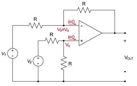
Determine $V_{OUT}$ as a function of $V_1$ and $V_2$ for the circuit shown below.

Denoting the non-inverting terminal of the op-amp as node a and the inverting terminal as node b, and applying the ideal op-amp rules results in the figure below:
The voltage $V_a$ can be determined from a voltage divider relation (or by applying KCL at node a) as $V_a = \frac{V_2}{2}$.
Thus, the voltage at the inverting terminal is $V_B = V_a = \frac{V_2}{2}$. Applying KCL at node b results in:
$$\frac{V_1-V_b}{R} = \frac{V_b-V_{OUT}}{R} \Rightarrow \frac{V_1 - \frac{V_1}{2}}{R} = \frac{frac{V_2}{2} - V_{OUT}}{R}$$
Simplification of the above results in $V_{OUT} = V_2 - V_1$.
Comments:
- The above circuit performs a subtraction operation. The voltage $V_1$ is subtracted from the voltage $V_2$.
- The inverting and non-inverting terminals of the op-amp are treated as separate nodes in this analysis, even though the op-amp constrains the voltages at these nodes to be the same. Thus, we apply KCL at each input terminal of the op-amp.
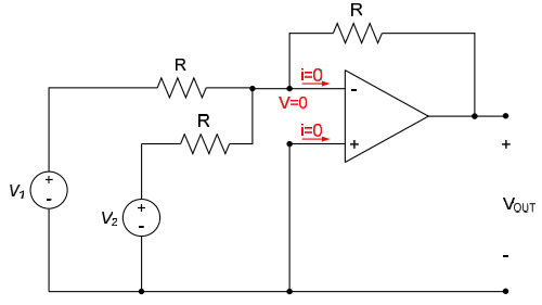
Example 5.4
Determine $V_{OUT}$ as a function of $V_1$ and $V_2$ for the circuit shown below.
Choosing the non-inverting terminal voltage as our reference voltage and applying the ideal operational amplifier rules allows us to label the voltages and currents shown in red below:
Applying KCL at the inverting terminal of the op-amp results in:
$$\frac{V_1-0}{R} + \frac{V_2 -0}{R} = \frac{0-V_{OUT}}{R}$$
Or
$$V_{OUT} = - \left( V_1 + V_2 \right)$$
Comments:
- The circuit inverts the sum of the inputs. One can use an inverting amplifier with a gain of one in conjunction with the above circuit to obtain a non-inverted sum of the inputs.
- An arbitrary number of inputs can be summed, by simply increasing the number of input signals and resistors applied at the inverting terminal of the op-amp, which is often referred to as the “summing node”.
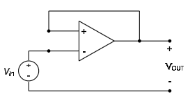
Example 5.5
Determine $V_{OUT}$ as a function of $V_{IN}$ for the circuit shown below.
Since there is no circuit element in the feedback loop, the inverting terminal voltage is identical to the output voltage, $V_{OUT}$. The ideal op-amp rules require that the inverting and non-inverting terminal voltages are the same, so:
$$V_{OUT} = V_{in}$$
The circuit is called a voltage follower, since the output voltage simply “follows” the input voltage. This circuit, though it appears to do nothing, is actually extremely useful. Since the input voltage is applied directly to an op- amp input terminal, the input resistance to the circuit is infinite and no current is drawn from the source. Thus, the source provides no power in order to generate the output voltage – all power provided to the load comes from the op-amp power supplies. This can be extremely useful in isolating different portions of a circuit from one another.
Consider, as an example, the following case. We have a loading circuit with an equivalent resistance of $100\Omega$. We wish to apply 6V to the circuit, but only have access to a 12V source. It is decided that we will use a voltage divider containing two $100\Omega$ resistors in series to reduce the supply voltage to the desired 6V level as shown in the circuit to the left below. However, adding the loading circuit to the voltage divider changes the voltage provided to the load, as shown to the right below.
Addition of a voltage follower to the circuit isolates the voltage divider from the load, as shown below. Power to the op-amp can be provided by connecting the 12V source to $V^+$ and grounding $V^-$, as shown, since the desired op-amp output is between 0V and 12V.
Section Summary
- Analysis of linear operational amplifier circuits typically consists of the following components:
- Assume that the voltage difference across the input terminals is zero.
- Assume that the currents into the input terminals is zero.
- Apply KCL at op-amp input terminals.
- Apply KCL at other circuit nodes, if necessary.
- Check to ensure that output voltage remains within range specified by op-amp power supply voltages.
- Op-amp circuits which perform the following functions are presented in this section:
- Inverting voltage amplification
- Non-inverting voltage amplification
- Summation (addition)
- Differencing (subtraction)
- Buffering
The reader should be able to sketch circuits, which perform the functions above.
Exercises
- Represent the circuit of Example 5.2 as a voltage controlled voltage source.
- Represent the circuit of Example 5.2 as a voltage controlled current source.
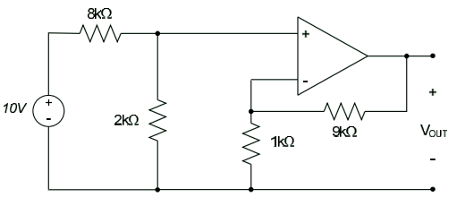
- Find $V_{out}$ for the circuit below
4. Find V in the circuit below.
5.5: Comparators
Operational amplifiers are intended to be incorporated into circuits which feeds back the op-amp output to one or both of the input terminals. That is, the output voltage is connected in some way to the op-amp inputs. Typically, for stable operation, the output is fed back to the inverting input terminal for stable operation (as in all of our circuit examples in section 5.4). If the output is not fed back to the input of the op-amp, the op-amp may not function as expected.
Comparators are operational amplifier –like devices which are intended to be operated without feedback from the output to the input. The circuit symbol for a comparator looks like an op-amp symbol, reflecting their similarities. Figure 5.15 provides a typical comparator symbol, with applicable voltages labeled.
Operation of the comparator is simple: if $v_p$ is greater than $v_n$, the output goes to the high supply voltage, $V^+$. If $v_p$ is less than $v_n$, the output goes to the low supply voltage, $V^-$. The comparator is essentially checking the sign between the voltage at the inverting and non-inverting inputs, and adjusting the output voltage accordingly. Mathematically, the operation of a comparator can be expressed as:
$$V_{OUT} = \begin{cases} V^+, v_p - v_n > 0\\ V^-, v_p - v_n < 0 \end{cases}$$
Because of this behavior, comparators are sometimes used to implement logical functions. Commercial comparators are also commonly equipped with a latch input. Once the latch is enabled, the output responds to only the time the polarity between the input terminal voltages changes.
Section Summary
- Unlike operational amplifiers, comparators are intended to operate without feedback.
- A comparator essentially operates on the difference in the voltage across the input terminals and puts out either a high or low voltage, depending upon the sign of the difference. The behavior of a comparator is typically modeled as:
$$V_{OUT} = \begin{cases} V^+, v_p - v_n > 0\\ V^-, v_p - v_n < 0 \end{cases}$$
Exercises
- A comparator like that shown in Figure 5.14 has the sinusoidal signal below applied across the input terminals. (E.g. the plot below is $v_p-v_n$ vs. time.) Sketch the output voltage $v_{out}(t)$.
5.6: A Few Non-ideal Effects
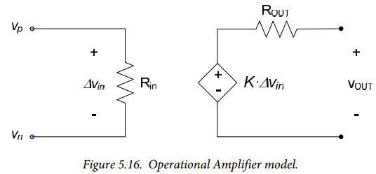
In section 5.2, we indicated that operational amplifiers are designed to have high input resistances, low output resistances and high gains between the input voltage difference and the output voltage. Figure 5.7 of section 5.2 provided a model of an operational amplifier as a dependent source, including input and output resistances. This model is repeated below as Figure 5.16 for convenience.
In section 5.2, we also provided the assumptions applicable to ideal operational amplifier operation, along with their associated conclusions, and are provided below:
- The output voltage is bounded by the power supply voltages: $V^- < v_{OUT} < V^+$
- $K \rightarrow \infty$. Thus, $\Delta v_{in} = 0$ and $v_p = v_n$
- $R_{in} \rightarrow \infty$. Thus, $i_p = -i_n = 0$, and the operational amplifier draws no power at its input.
- $R_{OUT} = 0$. Thus, there is no limit on the output current (or power) which can be provided by the op-amp.
Practical operational amplifiers have finite gains (K for most amplifiers is in the range $10^5 – 10^7$), finite input resistances (typical values are on the order of a few mega-ohms to hundreds or thousands of mega-ohms) and non-zero output resistances (generally on the order of 10 to 100 ohms). In this section, we will very briefly discuss a few of the ramifications of these non-ideal parameters.
Input Resistance Effects
The high input resistance of the operational amplifier means that circuits connected to the op-amp input do not have to provide much power to the op-amp circuit. This is the op-amp property that is employed in buffer amplifiers and instrumentation amplifiers. Instrumentation systems, for example, have very limited power output capabilities; these limitations are typically modeled as high output resistances in the instrumentation systems. Thermocouples, for example, provide low voltage levels, and very small power output – they can be modeled as a voltage source with a fairly high output resistance. When a system of this type is connected to the input terminals of an op-amp, the situation is as shown in Figure 5.17.
It is apparent from Figure 5.17 that the output resistance of the system, if it is large enough, can have an effect on the voltage difference across the op-amp input terminals, since:
$$\Delta v_{in} = V_S \left( \frac{R_{in}}{R_{in} + R_S} \right)$$
Since we generally want to amplify $V_S$ directly, any difference between $V_S$ and in $\Delta v_{in}$ will degrade our output voltage from its desired value.
Output Resistance Effects
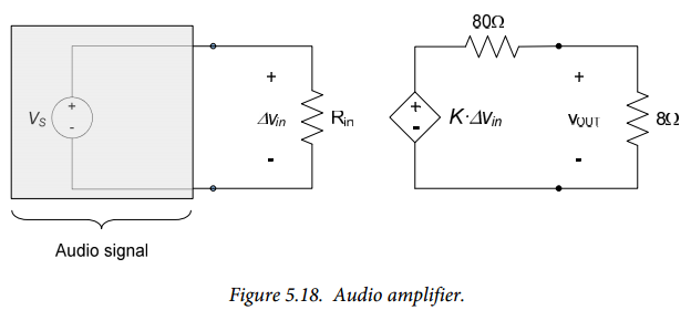
The op-amp output resistance essentially limits the amount of power the op-amp can provide at its output terminal. This can become a problem if we want to connect very low resistance loads to the output of an operational amplifier. For example, audio speakers commonly have an 8Ω resistance. Figure 5.18 shows an 8Ω speaker connected to the output of an operational amplifier which has an 80Ω output resistance. In this case, we expect the maximum output voltage to be:
$$v_{out} = K \cdot V_S \left( \frac{8\Omega}{8\Omega + 80\Omega} \right) = 0.09KV_s$$
If the maximum output voltage of the op-amp is low, we may not have nearly enough power to operate the speaker.
Finite Gain Effects
As an example of the effects of a finite voltage gain, let us assume that an operational amplifier has a gain of K = 10,000 and supply voltages $V^+ = 10V$ and $V^- = -10V$. From equation (5.2), the linear operating range of the operational amplifier is over the range of input voltage differences:
$$\frac{V^-}{K} \leq \Delta v_{in} \leq \frac{V^+}{K}$$
The non-ideal operational amplifier of interest can then allow input terminal voltage differences of up to $-1mV \leq \Delta v_{in} \leq 1mV$. Although voltage differences of a millivolt will be considered to be essentially zero for any of the voltage levels we will deal with in this class, these voltages are definitely not zero for some applications.
Section Summary
- The effect of a finite input resistance on an operational amplifier’s operation is that the current into the input terminals will not be identically zero. Thus, a real operational amplifier with finite input resistance will always draw some power from a circuit connected to it. Whether this has a significant effect on the overall circuit’s operation is generally a function of the output resistance of the circuit to which the amplifier is connected.
- The effect of a non-zero output resistance on an operational amplifier’s operation is that the power output of the amplifier is limited. Thus, a realistic operational amplifier will not be able to provide any arbitrary current to a load. Whether this has a significant effect on the overall circuit’s operation is primarily dependent upon the value of the load resistance.
- The effect of a finite op-amp gain is that the voltage difference across the input terminals may not be identically zero.


