JTAG SMT1 Reference Manual
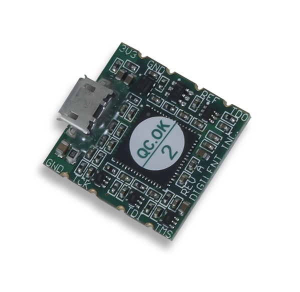

The JTAG-SMT1 is a compact, complete and fully self-contained surface-mount programming module for Xilinx FPGAs. It can be accessed directly from all Xilinx tools, including iMPACT, Chipscope, eFuse, Vivado and EDK. The module can be loaded directly onto a target board and reflowed like any other component.
The JTAG-SMT1 uses a 3.3V main power supply and a separate Vref supply to drive the JTAG signals. All JTAG signals use high speed, 24mA, three-state buffers that allow signal voltages from 1.8V to 5V and bus speeds of up to 30MBit/sec. JTAG signals are actively driven only during a programming event and are otherwise held in high-impedance, so the JTAG bus can be shared with other devices.

- Small, complete, all-in-one JTAG programming solution for Xilinx FPGAs
- Single 3.3V supply
- Separate Vref drives JTAG signal voltages; Vref can be any voltage between 1.8V and 5V.
- High-Speed USB2 port that can drive JTAG/SPI bus at up to 30Mbit/sec
- Able to drive JTAG bus at up to 30Mbit/sec
- JTAG/TCK frequency settable by user
- Compatible with all Xilinx tools
- Small form-factor surface-mount module can be directly loaded on target boards
- Uses micro-AB USB2 connector
- Same circuit is available as a stand-alone programming cable; see Digilent’s JTAG-HS1.
The SMT1 module is CE certified and fully compliant with the RoHS and REACH directives. It uses a standard Type-A to Micro-USB cable, also available from Digilent.
The JTAG signals can be connected directly to the corresponding FPGA signals as shown. For best results, the module should be mounted adjacent to the edge of the host PCB over a ground plane. Although signal traces may be run on top of the host PCB beneath the SMT1, it is recommended the area immediately beneath the SMT1 be kept clear. For highest speed JTAG operation, impedance between the SMT1 and FPGA should be kept below 100 Ohms.
Software Support
In addition to working seamlessly with all Xilinx tools, which includes iMPACT, Chipscope, eFuse, Vivado and EDK. The SMT1 is also supported by Digilent’s Adept software and the Adept SDK (the SDK can be freely downloaded from Digilent’s website). Adept includes a full-featured programming environment, and a set of public APIs that allow user applications to directly drive the JTAG chain.
Using the SDK, custom applications can be created to drive JTAG ports on virtually any device. The SDK also supports SPI ports, allowing applications to drive any SPI device using SPI Mode 0 or Mode 2. Please see the Adept SDK reference manual for more information.
Mechanical Information

Absolute Maximum Ratings
| Symbol | Parameter | Condition | Min | Max | Unit |
| Vdd | Operating supply voltage | -0.3 | 4.0 | V | |
| Vref | I/O reference/supply voltage | -0.3 | 6 | V | |
| VIO | Signal Voltage | -0.3 | 6 | V | |
| Iik,Iok | TMS, TCK, TDI, TDO, DC Input/Output Diode Current | VIO < -0.3V | -50 | mA | |
| VIO > 6V | +20 | ||||
| IOUT | DC Output Current | ±50 | mA | ||
| TSTG | Storage Temperature | -20 | +120 | ºC | |
| ESD | Human Body Model JESD22-A114 | 2000 | V | ||
| Charge Device Model JESD22-C101 | 500 | V | |||
DC Operating Characteristics
| Symbol | Parameter | Min | Typ | Max | Unit |
| Vdd | Operating supply voltage | 2.97 | 3.3 | 3.63 | Volts |
| Vref | I/O reference/supply voltage | 1.65 | 2.5/3.3 | 5.5 | Volts |
| TDO | Input High Voltage (Vih) | 0.75 x Vref | 5.5 | Volts | |
| Input Low Voltage (Vil) | 0 | 0.25 x Vref | Volts | ||
| TMS, TCK, TDI | Output High (Voh) | 0.85 x Vdd | 0.95 x Vdd | Vdd | Volts |
| Output Low (Vol) | 0 | 0.05 x Vdd | 0.15 x Vdd | Volts |
AC Operating Characteristics
SMT1 JTAG signals are driven according to the timing diagram below. JTAG/TCK frequencies from 30MHz to 8KHz are supported, at integer divisions of 30MHz from 1 to 3750. Common frequencies include 30MHz, 15MHz, 10MHz, 7.5MHz, and 6HMz. JTAG/TCK operating frequency can be set from within the Xilinx tools – please refer to Xilinx’s iMPACT documentation for more information.

| Symbol | Parameter | Min | Max |
| Tck | Tck period | 33ns | 2.185ms |
| Tckh, Tckl | Tclk pulse width | 20ns | 1.1ms |
| Tcd | Tclk to TMS, TDI | 0 | 15ns |
| Tsu | TDO Setup time | 19ns | |
| Thd | TDO Hold time | 0 |
Mounting to Host PCBs
The JTAG-SMT1 module has a moisture sensitivity level (MSL) of 6. Prior to reflow, the JTAG-SMT1 module must be dried by baking it at 70° C for 72 hours (the tray and the module itself can be baked 125° C for 24 hours, but any labels and rubber feet present on the module cannot withstand this higher temperature). Once this process has been completed, the module has a MSL of 3 and is suitable for reflow for up to 168 hours without additional drying.
SMT1 signal pads are finished with the ENIG process using 2u” gold over 150u” electroless nickel. The SMT1 is compatible with most mounting and reflow processes. The binding force of the solder is sufficient to hold the SMT1 firmly in place; no additional adhesives are required.

Packaging
Small quantities (less than 20 per order) will be individually packaged in antistatic bags for shipping. Larger quantities will be packed in 80 position antistatic bubble trays.
