DSDB Programming Guide
This section demonstrates how to create a LabVIEW project and FPGA VI that performs the following:
- Routes switch SW0 to LED0, which causes LED0 to light when switch SW0 is moved to the ON position, and turn off when the switch moved to the OFF position.
- Routes push button BTN0 to LED2, which causes LED2 to light when button BTN0 is pressed, and turn off when the button is depressed.
This example also demonstrates how to compile and run the FPGA VI on the DSDB.
Prerequisites
Hardware
- DSDB
Software
- LabVIEW 2015 SP1 or newer
- LabVIEW FPGA
- NI Xilinx Tools
- NI-DSDB
Procedure
To begin programming with LabVIEW, connect the USB cable to the DSDB, apply power to the board, and move the power switch to the ON position.
Creating a Project
- Launch LabVIEW.
- In the Getting Started window, click Empty Project. The new project opens in the Project Explorer window.
- Save the project as FPGA_Design.lvproj.
Creating an FPGA Target VI
- In the Project Explorer window, right-click My Computer and select New»Targets and Devices.
- In the Add Targets and Devices on My Computer window, select New target or device, expand Digilent, and highlight Digital Systems Development Board. Click OK. The target is discovered and the target and target properties are loaded into the project tree.
- In the Project Explorer window, right-click FPGA Target (DSDB, Digital Systems Development Board), and select New»VI. A blank VI opens. Select the block diagram window.
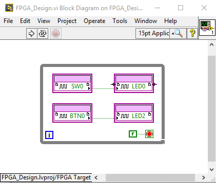
- In the Project Explorer window FPGA Target (DSDB, Digital Systems Development Board) tree view, select SW0 and LED0 and drag them onto the block diagram as shown in the image below.
- In the LabVIEW block diagram, wire SW0 output to the LED0 input.
- In the Project Explorer window FPGA Target (DSDB, Digital Systems Development Board) tree view, select BTN0 and LED2 and drag them onto the block diagram.
- In the LabVIEW block diagram, wire BTN0 output to the LED2 input.
- Add a While Loop around the resources.
- Wire a false constant to the stop condition of the While Loop as shown below.
- Save the VI as FPGA_Design.vi.
Running the FPGA VI
- Verify that the USB cable is connected to the DSDB and host PC, and the power switch is moved to the ON position.
- Open the front panel of FPGA_Design.vi.
- Click the Run button to run the VI.
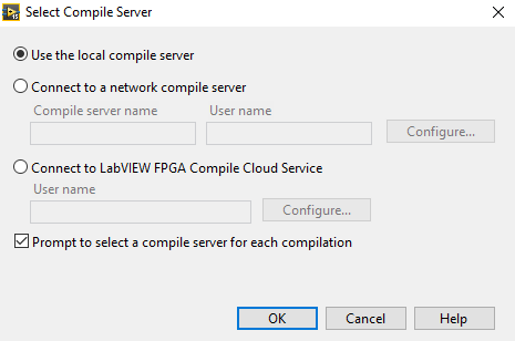
- The application compiles VHDL code and generates a bitstream file that is downloaded into the FPGA configuration storage. The Generating Intermediate Files window opens and displays the compilation progress. The LabVIEW FPGA Compile Server window opens and runs. Choose compile locally. The compilation takes several minutes. See an image of the compile server window below.
- When the compilation finishes, click the Stop Server button to close the LabVIEW FPGA Compile Server.
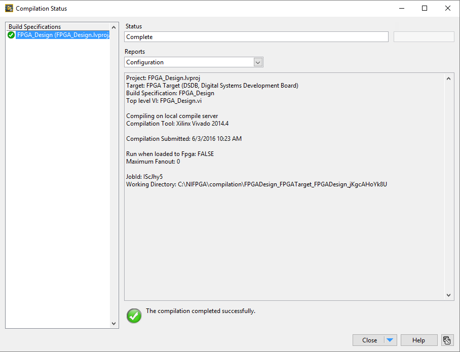
- Click Close in the Successful Compile Report window as shown in the image below.
- The application is running on the FPGA board at this time.
- Move switch SW0 up and down; LED0 should correspondingly light and turn off.
- Press button BTN0; LED2 should correspondingly light and turn off.
More DSDB examples can be found in the LabVIEW Example Finder.
- In LabVIEW Click Help»Find Examples.
- Click the Search tab.
- Search for 'dsdb'.
- Open one of the provided examples and follow the included instructions.


