chipKIT™ Max32™

Revision History
March, 2015
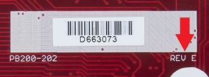
This document applies to REV E of the board, as indicated on the underside next to the barcode.
Overview
The chipKIT Max32 is a microcontroller board based on the Microchip PIC32MX795F512L, a member of the 32-bit PIC32 microcontroller family.
The Max32 is the same form factor as the Arduino™ Mega board and is compatible with many Arduino shields as well as larger shields for use with the Mega boards. It features a USB serial port interface for connection to the IDE and can be powered via USB or an external power supply.
The Max32 is easy to use and suitable for both beginners and advanced users experimenting with electronics and embedded control systems.
It was designed to be programmed using the Multi-Platform Integrated Development Environment (MPIDE), an environment based on the original Arduino IDE and modified to support PIC32. It contains everything needed to start developing embedded applications. The Max32 can also be programmed, and debugged, with Microchip's MPLAB® X IDE development tool using a licensed debugger/programmer such as the chipKIT PGM or the PICkit®3.
The Max32 has 83 I/O pins that support a number of peripheral functions, such as UART, SPI, and I2C ports and pulse width modulated outputs. Sixteen of the I/O pins can be used as analog inputs or as digital inputs and outputs.
The PIC32 microcontroller on the Max32 also provides a 10/100 Ethernet MAC, USB 2.0 full-speed OTG controller, and two CAN controllers. An add-on board like the chipKIT Network Shield is needed to use these advanced peripherals.
The Max32 can be powered via USB, an external AC-DC power adapter, or batteries.
Features include:
- a Microchip® PIC32MX795F512L microcontroller (80Mhz, 512K Flash, 128K RAM)
- 3.3V operating voltage
- 90mA typical operating current
- 7V to 15V input voltage (recommended)
- 20V input voltage (maximum)
- 83 available I/O pins
- 16 analog inputs
- 0V to 3.3V analog input voltage range
- +/-18mA DC current per pin
- a 10/100 Ethernet MAC
- a USB 2.0 full-speed OTG controller
- 2 CAN controllers
1 Hardware Overview
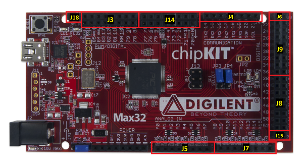
The Max32 board has the following hardware features:
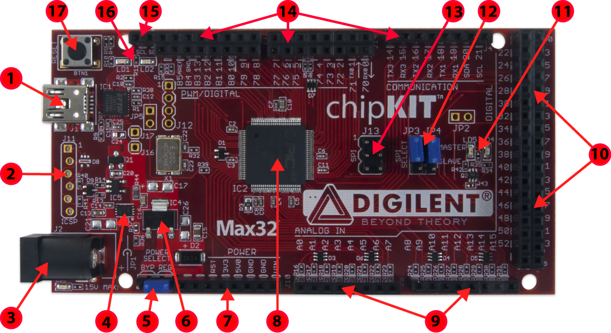
1. USB Connector for USB Serial Converter
This connects to a USB port on the PC to provide the communications port for the MPIDE to talk to the Max32 board. This can also be used to power the Max32 board when connected to the PC.
2. J11: Microchip Debug Tool Connector
This connector is used to connect Microchip programmer/debugger tools, such as the PICkit™3. This allows the Max32 board to be used as a traditional microcontroller development board using the Microchip MPLAB® IDE.
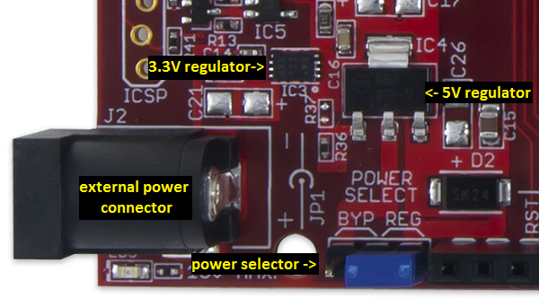
3. J2: External Power Connector
This is used to power the Max32 board from an external power supply. This is a 5.5mm x 2.1mm barrel connector. It is wired with the center terminal as the positive supply voltage. The power supply voltage must be in the range 7V to 15V.
4. Power Supply – 3.3V Regulator
Voltage regulator for the 3.3V power supply. This power supply can provide up to 500mA of current.
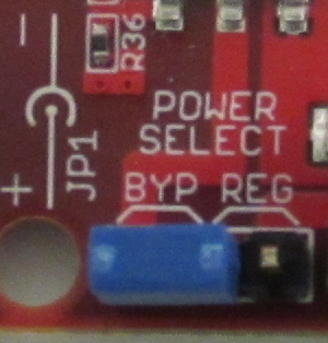
5. JP1: Power Select Jumper
This jumper is used to route power from the external power connector through the on-board 5V voltage regulator or to bypass the 5V regulator. The REG position routes power through the 5V regulator. The BYP position bypasses the on-board 5V regulator. With this jumper in the BYP position the maximum input voltage that can be applied at the external power connector is 6V.
6. Power Supply – 5V Regulator
This on-board 5V voltage regulator regulates the input voltage applied at the external power connector to 5V. This is used to power the 3.3V regulator and to provide 5V power to expansion shields. This regulator can provide up to 800mA of current.
7. J10: Shield Power Connector
This connector provides power to I/O expansion shields connected to the board.
8. PIC32 Microcontroller
The PIC32MX795F512L microcontroller is the main processor for the board.
9. J5, J7: Analog Signal Connectors
These connectors provide access to analog/digital I/O pins on the microcontroller.
10. J6, J8, J9, J15: Digital Signal and Power Connectors
These are shown as four connectors in the Max32 schematic. There is a single connector loaded across all four when the board is assembled. These provide 5V power, ground, and access to digital I/O pins on the microcontroller to shields connected to the board.
11. User LEDs
Two user LEDs. LD4 is connected to digital signal pin 13. LD5 is not connected to any external digital signal pin, but both LEDs can be accessed in MPIDE using the macros PIN_LED1 (LD4) and PIN_LED2 (LD5).
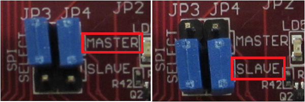
12. JP3 & JP4: SPI Master/Slave Select Jumpers
These jumpers are used to switch the SPI signals for use of the Max32 board as an SPI master device or as an SPI slave device. Both jumpers should be switched together. Place the shorting blocks in the MASTER position for master operation and in the SLAVE position for slave operation. Normally, these jumpers are in the MASTER position.
13. J13: SPI Signal Connector
This connector provides alternative access to the SPI signals. This is used by some shields for access to the SPI bus.
14. J3, J4, J14: Digital Signal Connectors
These connectors provides access to digital I/O pins on the microcontroller.
15. J18 - I²C
Dedicated I²C signals. These signals are connected directly to I2C1 on the microcontroller and are shared with pins 20 and 21 on connector J4.
16. Communications Status LEDs
These LEDs indicate activity on the USB serial interface.
17. Reset Button
This button can be used to reset the microcontroller, restarting operation from the boot loader.
2 Jumper Settings
The chipKIT development platforms use a Microchip PIC32 microcontroller. These are 32-bit products that bring unprecedented features to the Arduino community. In order to maintain compatibility with existing hardware and software, additional jumpers and row headers are provided.
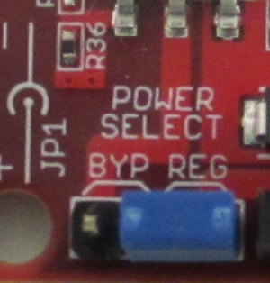 JP1 Used in conjunction with an external DC power supply of 7V-15V connected to J2. Placing the shorting block in the REG position will force the input voltage from the power connector J2 to pass through the 5V voltage regulator IC4. This regulated 5V output is then tied to the VCC5V0 bus. It is also used to power the 3.3V regulator IC3. The VIN bus will have the same potential as the external power supply. This should also be the default position if you are unsure.
Placing the shorting block in the BYP position bypasses the 5V regulator IC4 and ties directly to the VCC5V0 bus and also powers the 3.3V regulator IC3. It is not recommended to connect more than 6V external power through the power connector J2 when JP1 is in the BYP position.
 When powering the board from only the USB, placing the shorting block in the REG position will disconnect the VIN bus. Placing the shorting block in the BYP position will tie the VIN bus to the VCC5V0 and USB5V0 busses. Power limitations on the USB5V0 bus will apply the VIN bus in this case.
The Max32 can be connected to both a 5V USB power source and an external power source of 7V or more. Place the shorting block in the REG position in this case.
For more information on power supplies, see section 5 Power Supply below.
JP3 & JP4 Used in conjunction with SPI connector J13. The chipKIT Max32 can be configured as either a Master device or Slave device according to standard SPI protocol. Both shorting blocks should be moved together when switching between Master and Slave. Data flow will also swap depending on the position of the shorting blocks.

3 chipKIT Max32 Hardware Description
3.1 MPIDE and USB Serial Communication
The Max32 board is designed to be used with the Multi-Platform IDE (MPIDE). Digilent produced the MPIDE development platform by modifying the Arduino IDE. It is fully backwards-compatible with the Arduino IDE.
The MPIDE uses a serial communications port to communicate with a boot loader running on the Max32 board. The serial port on the Max32 board is implemented using an FTDI FT232R USB serial converter. Before attempting to use the MPIDE to communicate with the Max32, the appropriate USB device driver must be installed, which should happen automatically the first time you connect your Max32 to your PC. The Max32 board uses a standard mini-USB connector for connection to a USB port on the PC.
When the MPIDE needs to communicate with the Max32 board, the board is reset and starts running the boot loader. The MPIDE then establishes communications with the boot loader and downloads the program to the PIC32795. When the MPIDE opens the serial communications connection on the PC, the DTR pin on the FT232R chip is driven low. This pin is coupled through a capacitor to the MCLR pin on the PIC32 microcontroller. Driving the MCLR line low resets the microcontroller, restarting execution with the boot loader. This automatic reset action (when the serial communications connection is opened) can be disabled. To disable this operation, there is a cuttable trace on the bottom of the board between the pins on JP5. JP5 is normally not loaded. If the trace between the pins on JP5 has been cut, the automatic reset operation can be restored by loading JP5 and inserting a shorting block across it. It should be noted that the reset button on the board and the reset pin on the shield power connecter (J10) are both independent of JP5 and will still force the PIC32 microcontroller to reset.
Two red LEDs (LD1 and LD2) will blink when data is being sent or received between the Max32 and the PC over the serial connection.
The header connector J12 provides access to the other serial handshaking signals provided by the FT232R. Connector J12 is not loaded at the factory and can be loaded by the user to access these signals.
3.2 Power Supply
The Max32 is designed to be powered either via USB or from an external power supply. There is an automatic switchover circuit that causes the external supply to be used if both supplies are present.
The power supply section in the Max32 uses two voltage regulators. The first regulates the external voltage to 5V to power the VCC5V0 bus. The second regulates the VCC5V0 bus to 3.3V to provide power to the VCC3V3 bus that powers the PIC32 microcontroller.
The 5V voltage regulator is normally an NCP1117. The board is designed to be able to also use an LM1117, but the NCP1117 is the part normally used. The NCP1117 is rated for an output current of 1A (the LM1117 is rated for 800mA). The dropout voltage of the NCP1117 is a maximum of 1.2V at the rated output current (1.3V for the LM1117).
There is a reverse-polarity protection diode in the external power supply circuit. Considering the diode drop plus the forward drop across the regulator, the minimum input voltage to the regulator should be 7V to produce a reliable 5V output. The absolute maximum input voltage of both the NCP1117 and the LM1117 is 20V. The recommended maximum operating voltage is 15V.
For input voltages above 9V, the regulator will get extremely hot when drawing high currents. Both the NCP1117 and the LM1117 have output short circuit protection and internal thermal protection and will shut down automatically to prevent damage.
The 3.3V regulator is a Microchip MCP1725. This regulator is rated for a maximum output current of 500mA. The absolute maximum input voltage for the MCP1725 is 6V. This regulator has internal short circuit protection and thermal protection. It will get noticeably warm when the current consumed by the VCC3V3 bus is close to the 500mA maximum.
The 5V power bus VCC5V0 can be powered from one of three sources:
- the USB5V0 bus when the board is operating under USB power
- the output of the on-board 5V regulator when operating from an external 7V – 15V supply
- directly from the external supply when operating from a regulated 5V external supply with jumper JP1 in the BYP position.
Switch-over from USB power to external power is done automatically and the external supply will be used if both are present.
Jumper JP1 is used to route the external power supply voltage through the on-board 5V regulator or directly to the VCC5V0 bus, bypassing the on-board 5V regulator. Normally, JP1 is in the REG position. This routes the external supply through the 5V regulator. Operation from an externally regulated 5V supply is provided by placing the jumper in the BYP position.
The forward drop across the MCP1725 is typically 210mV (350mV max) at 500mA output. With JP1 in the BYP position, this will allow correct operation of the 3.3V power supply from an input voltage down to 3.5V. This lets you power the board from batteries and other lower voltage power sources. In that case, the VCC5V0 power bus will not be powered at 5V.
Note: When JP1 is in the BYP position, do not apply more than 6V to the external power input. It can destroy the 3.3V regulator and possibly the PIC32 microcontroller as well.
The PIC32 microcontroller is rated to use a maximum of 98mA of current when operating at 80Mhz. This allows up to ~400mA from the VCC3V3 bus and up to 700mA from the VCC5V0 bus to power external devices.
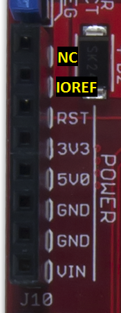 The POWER connector J10 is used to provide power to shields connected to the Max32 board. The following pins are provided on this connector:
- NC (pin 1): This pin is not used.
- IOREF (pin 2): Provides a 3.3v reference voltage to the shield which the shield should observe as the maximum input pin voltage to the Max32.
- P32_MCLR (pin 3): This connects to the MCLR pin on the PIC32 microcontroller and can be used to reset the PIC32.
- VCC3V3 (pin 4): This routes the 3.3V power bus to shields. This pin can provide ~400mA.
- VCC5V0 (pin 5): This routes the 5V power bus to shields. This pin can provide up to ~700mA to shields, however the total provided by pins 2 and 3 shouldn't exceed 800mA.
- GND (pin 6, 7): This provides a common ground connection between the Max32 and the shields.
- VIN (pin 8): This connects to the voltage provided at the external power supply connector. This can be used to provide unregulated input power to the shield. It can also be used to power the Max32 board from the shield instead of from the external power connector.
3.3 5V Compatibility
The PIC32 microcontroller operates at 3.3V. The original Arduino boards operate at 5V, as do many Arduino shields.
There are two issues to consider when dealing with 5V compatibility for 3.3V logic. The first is protection of 3.3V inputs from damage caused by 5V signals. The second is whether the 3.3V output is high enough to be recognized as a logic high value by a 5V input.
The digital I/O pins on the PIC32 microcontroller are 5V tolerant. The analog capable I/O pins are not 5V tolerant. However, To provide 5V tolerance on those pins, the Max32 contains clamp diodes and current-limiting resistors to protect them from 5V input voltages. The fact that all I/O pins on the Max32 are 5V tolerant means that it is safe to apply 5V logic levels to any pins on the board without risk of damaging the PIC32 microcontroller.
The minimum output high voltage of the PIC32 microcontroller is rated at 2.4V when sourcing 12mA of current. When driving a high impedance input (typical of CMOS logic) the output high voltage will be close to 3.3V. Some 5V devices will recognize this voltage as a logic high input, and some won’t. Many 5V logic devices will work reliably with 3.3V inputs.
3.4 Input/Output Connections
 The Max32 board provides 83 of the I/O pins from the PIC32 microcontroller to pins on the input/output connectors J3, J4, J5, J7, J8, J9, and J14.
The PIC32 microcontroller can source or sink a maximum of 18mA on all digital I/O pins. However, to keep the output voltage within the specified voltage range (VOL 0.4V, VOH 2.4V) the pin current must be restricted to +7/-12mA. The maximum current that can be sourced or sunk across all I/O pins simultaneously is +/- 200mA. The maximum voltage that can be applied to any I/O pin is 5.5V. For more detailed specifications, refer to the PIC32MX5XX/6XX/7XX data sheet available from www.microchip.com.
Connectors J3, J8, J9, and J14 are 2×8 female pin header connectors that provide digital I/O signals. Connector J4 is a 1×8 female pin header that provides digital I/O signals as well as UART1-3 and I²C communication signals. J18 is a 1×2 female pin header next to LD1 and LD2 that provides additional connection to the I²C signals. Connectors J5 and J7 are 1×8 female pin headers that provide analog inputs as well as digital I/O signals.
Connectors J6 and J15 are two-pin headers that provide power and ground to shield boards. J6 provides two pins connected to the VCC5V0 bus and J15 provides two pins connected to GND.
Note that although J6, J8, J9 and J15 are shown as separate connectors on the schematic, a single 2×18 connector is loaded across all of them when the board is manufactured.
On connectors J3 and J14, the outer row (closer to the board edge) of pins corresponds to the I/O connector pins on an Arduino Mega or Mega 2560 board. The inner row of pins provides access to the extra I/O signals provided by the PIC32 microcontroller.
The chipKIT/Arduino system uses logical pin numbers to identify digital I/O pins on the connectors. The logical pin numbers for the I/O pins on the Max32 are 0 – 85 and are labeled in the silk screen on the board.
The analog inputs on connectors J5 and J7 are also assigned digital pin numbers. Pins A0 – A7 on connector J5 are digital pins 54 – 61, and pins A8 – A15 on connector J5 are digital pins 62 – 69.
Pin numbers 70 – 85 are on the inner rows of connectors J14 and J3.
3.5 Peripheral I/O Functions
The PIC32 microcontroller on the Max32 board provides a number of peripheral functions. The following peripherals are provided:
UART port 0
Asynchronous serial port. Pin 0 (RX0), Pin 1 (TX0). These pins are connected to I/O connector J14 and are also connected to the FT232R USB serial converter. It is possible to use these pins to connect to an external serial device when not using the USB serial interface. This uses UART1A (U1ARX, U1ATX) on the PIC32 microcontroller.
UART port 1
Asynchronous serial port. Pin 19 (RX1), Pin 18 (TX1) on connector J4. This uses UART1B (U1BRX, U1BTX) on the PIC32 microcontroller.
UART port 2
Asynchronous serial port. Pin 17 (RX2), Pin 16 (TX2) on connector J4. This uses UART3A (U3ARX, U3ATX) on the PIC32 microcontroller.
UART port 3
Asynchronous serial port. Pin 15 (RX3, Pin 14 (TX3) on connector J4. This uses UART3B (U3BRX, U3BTx) on the PIC32 microcontroller.
SPI
Synchronous serial port. Pin 53 (SS), Pin 51 (MOSI), Pin 50 (MISO), Pin 52 (SCK). This uses SPI2A (SS2A, SDI2A, SDO2A, SCK2A) on the PIC32 microcontroller. These signals also appear on connector J13. Jumpers JP3 and JP4 are used to select whether the Max32 operates as a Master (transmit on MOSI, receive on MISO) or a Slave (transmit on MISO, receive on MOSI) device. The shorting blocks on JP3 and JP4 are normally placed in the Master position for the Max32 to function as an SPI master.
I²C
Synchronous serial interface. These signals are available on J18 and are shared with pins 21 (SCL) on and pin 20 (SDA) on connector J4. This uses I2C1 (SDA1, SCL1) on the PIC32 microcontroller.
Note: The I²C bus uses open collector drivers to allow multiple devices to drive the bus signals. This means that pull-up resistors must be provided to supply the logic high state for the signals. These pull-up resistors are not on the Max32 board and must be provided externally. The resistance of the pull-up resistor to use depends on the total number of devices on the bus, the length of wire, and the clock speed being used. It essentially depends
on distributed capacitance on the bus. The higher the distributed capacitance and the faster the clock speed, the smaller the resistance should be. Values typically used are in the range of 2K to 10K ohms.
PWM
Pulse width modulated output. Pins 3 (OC1), 5 (OC2), 6 (OC3), 9 (OC4), and 10 (OC5).
External Interrupts
Pin 3 (INT0), Pin 2 (INT1), Pin 7 (INT2), Pin 21 (INT3), Pin 20 (INT4).
User LEDs
Two user LEDs are provided, Pin 13 (LD4) and Pin 86 (LD5). Pin 13 is shared between a connector and LD4. Pin 86 is dedicated to LD5 and is not shared with any connector pin. Driving the pin high turns the LED on, driving it low turns it off.
A/D Converter Reference
Labeled A, the leftmost outer pin on connector J3. This is used to provide an external voltage reference to determine the input voltage range of the analog pins. The maximum voltage that can be applied to this pin is 3.3V. Note that this signal is duplicated on connector J8 and corresponds to digital I/O pin 44. If the A pin is being used as an analog reference, then pin 44 is not usable.
RESET
The PIC32 microcontroller is reset by bringing its MCLR pin low. The MCLR pin is connected to the P32_RST net on the circuit board.
As described above, resetting the PIC32 microcontroller can be initiated by the USB serial converter. The USB serial converter brings the DTR pin low to reset the microcontroller. Jumper JP5 can be used to enable/disable the ability for the USB serial converter to initiate a reset.
The P32_RST net is connected to pin 3 of power connector J10. This allows circuitry on a shield to reset the microcontroller, or to ensure that the circuitry on the shield is reset at the same time as the microcontroller.
Connector J13 provides access to the SPI bus. Pin 5 provides access to the SPI Slave Select signal (SS).
On Arduino boards, the corresponding connector is also used as an in-system programming connector as well as providing access to some of the SPI signals. On Arduino boards, pin 5 of this connector is connected to the reset net.
Some Arduino shields, notably, the Ethernet shield, connect J13 pin 5 to the reset net on pin 1 of connector J10. This causes the processor to be reset each time an attempt is made to access the SPI port. Jumper JP2 can be used to break the connection between J13 pin 5 and reset when using Arduino shields that make this connection. JP2 has a cuttable trace on the bottom of the board that can be cut to break the connection between SPI SS and reset. JP2 is not loaded at the factory. To restore the connection, solder a 2-pin header at the JP2 position and install a shorting block.
A reset button is at the upper left corner of the board. Pressing this button will reset the PIC32 microcontroller.
RTCC
Real-time clock/calendar. The PIC32 microcontroller contains an RTCC circuit that can be used to maintain time and date information. The operation of the RTCC requires a 32.768Khz frequency source. Pin 75 (SOSCI) is the clock input for the RTCC. A 32.768Khz oscillator should be connected to this pin to allow use of the RTCC.
See the pinout diagram and tables in the appendices for a complete list of pin functions.
3.6 Advanced Peripheral Devices
The PIC32MX795F512L microcontroller on the Max32 board has several peripheral devices for advanced communications capabilities. These peripheral devices require additional hardware that isn’t provided on the Max32 board. This additional hardware must be provided by a shield board (such as the Digilent chipKIT Network Shield) connected to the Max32.
These advanced peripheral functions make use of various I/O pins for their operation. Most of the I/O pins used by the advanced peripheral devices are located on connectors J8 and J9. When these pins are being used by the advanced peripheral functions they are not available for other uses.
USB: The USB OTG controller allows using the Max32 board to implement a USB device, USB host, or USB OTG host/device. The following pins are used by the USB interface: Pin 27 (D+), Pin 26 (D-), Pin 25 (USBID), Pin 24 (VBUS).
Pin 24 (VBUS) can be used by a self-powered USB device to monitor the presence of bus voltage on the USB bus. This pin on the PIC32 microcontroller is an analog input pin used by the USB controller, and is not usable as a user I/O pin even when not using the USB controller.
10/100 Ethernet MAC: The Ethernet MAC requires an external PHY to complete the implementation of an Ethernet network port. The Ethernet MAC constructs the digital format of packets being sent and performs the checking and buffering of packets being received. The PHY provides the physical interface and translates the digital signals used by the MAC into the analog voltages used on the Ethernet cable.
There are two common interfaces used between an Ethernet MAC and the PHY: MII and RMII. The MAC in the PIC32 supports either interface, but the Max32 board is designed to use the RMII interface. The RMII Ethernet PHY interface uses the following pins: Pin 53 (EREFCLK), Pin 49 (EMDC), Pin 48 (EMDIO), Pin 47 (ETXEN), Pin 46 (ETXD0), 45 (ETXD1), Pin 43 (ECRSDV), Pin 42 (ERXD0), Pin 41 (ERXD1), Pin 40 (ERXERR), and Pin 7 (NRST).
CAN1, CAN2: The CAN controllers allow the Max32 to participate in one or two CAN (Controller Area Network) networks. CAN is a networking standard that was developed for use in the automotive industry and is now also use in building automation and other industrial applications. The CAN controllers in the PIC32 microcontroller require external CAN transceivers to connect to the network wiring.
The CAN1 interface uses the following pins: Pin 15 (AC1RX), Pin 14 (AC1TX). Note that these pins are also used by UART3.
The CAN2 interface uses the following pins: Pin 23 (AC2RX), Pin 22 (AC2TX).
The PIC32 microcontroller is designed to allow one of two sets of pins to be used by the CAN controllers to connect to the transceivers. The Max32 board is designed to use the alternate sets of pins.
3.7 Microchip Development Tool Compatibility
In addition to being used with the MPIDE, the Max32 board can be used as a more traditional microcontroller development board using Microchip Development Tools.
Unloaded connector J11 on the left side of the board is used to connect to a licensed Microchip development tool, such as the chipKIT PGM or the PICkit™3. The holes for JP3 are staggered so that a standard 100-mil-spaced 6-pin header can be press fit to the board without the need to solder it in place. Any Microchip development tool that supports the PIC32 microcontroller family, and can be connected via the same 6-pin interface as the PICkit3, can be used. Additional considerations from user danmcb
 Typically, a right-angle male connector is used in J11 so that the programmer can be attached co-planar with the Max32 board. Whichever way the right-angle connector is loaded, be sure to match pin 1 on the programmer's connector with pin 1 (square solder pad) on J11. Connecting the programmer incorrectly may cause damage to the PIC32 microcontroller or programmer. When using the PGM or the PICkit™3, there is a small white arrow indicating pin 1.
If J11 is loaded from the top, the PICkit3 will interfere with the USB connector and the external power connector. A short six-wire cable can be used between the PICkit3 and the Max32. If J11 is loaded from the bottom, the PICkit3 won’t interfere with the USB and external power connectors.
The Digilent PICkit3 Programming Cable Kit includes all necessary connectors and a cable for connecting a PICkit3 to the Max32.
The Microchip MPLAB® IDE or the MPLAB® X IDE can be used to program and debug code running on the Max32 board. These programs can be downloaded from www.microchip.com.
4 Reloading the MPIDE bootloader
Using the Microchip development tools to program the Max32 board will cause the boot loader to be erased. To use the board with the MPIDE again, it is necessary to program the boot loader back onto the board. The boot loader source code and compiled image can be found in the MPIDE software download. Once you have the boot loader .hex file, complete the following steps to reload the boot loader to the PIC32 microcontroller using MPLAB® X.
- Open MPLAB X. Click on “File”, highlight “Import”, and then click “HEX/ELF…(Prebuilt) File”
- Click on “Browse”and search for the arduino-bootloader.X.Max32.hex file you downloaded from the webpage. (If you have more than one board from the chipKIT family, it may be helpful to store all of your applicable boot loaders in one common file.)
- Select “32-bit MCUs (PIC32)” in the “Family:” dialog box. Then select the device ID “PIC32MX795F512L” in the “Device:” dialog box.
- Make sure your programmer device is connected and selected in the “Hardware Tool” box at the bottom. (It is not necessary to have the programmer connected in order to build the project, but it must be connected in order to load the boot loader to the microcontroller.)
- Click “Next” when the correct options have all been chosen.
- Rename the project if you wish. The name of the .hex file is used by default.
- Choose where to place your project. The file where your boot loader is located is used by default.
- Click “Finish” to finalize the project file.
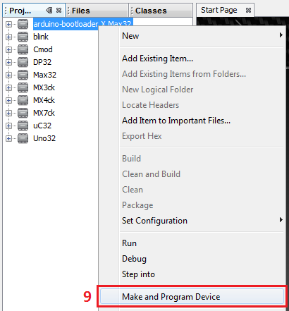
- The project will pop up in the “Projects” tab on the left side of the screen. With the programmer connected, right-click the project name and select “Make and Program Device”. The boot loader will now load to the microcontroller. (You may also click the button on the tool bar with the green arrow pointing down to load the project if the project has been set as the main project.)
Appendix A: Pinout Tables
Pinout Table by Logical Pin Number
| chipKIT Pin # | Connector Pin # | PIC32 Pin # | PIC32 Signal | Notes |
|---|---|---|---|---|
| 0 | J14-01 | 52 | SDA1A/SDI1A/U1ARX/RF2 | |
| 1 | J14-03 | 53 | SCL1A/SDO1A/U1ATX/RF8 | |
| 2 | J14-05 | 18 | AERXD0/INT1/RE8 | |
| 3 | J14-07 | 72 | SDO1/OC1/INT0/RD0 | |
| 4 | J14-09 | 74 | SOSCO/T1CK/CN0/RC14 | |
| 5 | J14-11 | 76 | OC2/RD1 | |
| 6 | J14-13 | 77 | OC3/RD2 | |
| 7 | J14-15 | 19 | AERXD1/INT2/RE9 | |
| 8 | J3-01 | 79 | ETXD2/IC5/PMD12/RD12 | |
| 9 | J3-03 | 78 | OC4/RD3 | |
| 10 | J3-05 | 81 | OC5/PMWR/CN13/RD4 | |
| 11 | J3-07 | 9 | T5CK/SDI1/RC4 | |
| 12 | J3-09 | 58 | SCL2/RA2 | |
| 13 | J3-11 | 59 | SDA2/RA3 | |
| 14 | J4-08 | 39 | AC1TX/SCK3A/U3BTX/U3ARTS/RF13 | |
| 15 | J4-07 | 40 | AC1RX/SS3A/U3BRX/U3ACTS/RF12 | |
| 16 | J4-06 | 50 | SCL3A/SDO3A/U3ATX/PMA8/CN18/RF5 | |
| 17 | J4-05 | 49 | SDA3A/SDI3A/U3ARX/PMA9/CN17/RF4 | |
| 18 | J4-04 | 48 | AETXD1/SCK1A/U1BTX/U1ARTS/CN21/RD15 | |
| 19 | J4-03 | 47 | AETXD0/SS1A/U1BRX/U1ACTS/CN20/RD14 | |
| 20 | J4-02, J18-02 | 67 | AETXEN/SDA1/INT4/RA15 | |
| 21 | J4-01, J18-01 | 66 | AETXCLK/SCL1/INT3/RA14 | |
| 22 | J9-16 | 7 | T3CK/AC2TX/RC2 | |
| 23 | J9-15 | 8 | T4CK/AC2RX/RC3 | |
| 24 | J9-14 | 54 | VBUS | |
| 25 | J9-13 | 51 | USBID/RF3 | |
| 26 | J9-12 | 56 | D-/RG3 | |
| 27 | J9-11 | 57 | D+/RG2 | |
| 28 | J9-10 | 1 | AERXERR/RG15 | |
| 29 | J9-09 | 11 | ECRX/SDA2/SDI2A/U2ARX/PMA4/CN9/RG7 | |
| 30 | J9-08 | 5 | PMD7/RE7 | |
| 31 | J9-07 | 4 | PMD6/RE6 | |
| 32 | J9-06 | 3 | PMD5/RE5 | |
| 33 | J9-05 | 100 | PMD4/RE4 | |
| 34 | J9-04 | 99 | PMD3/RE3 | |
| 35 | J9-03 | 98 | PMD2/RE2 | |
| 36 | J9-02 | 94 | PMD1/RE1 | |
| 37 | J9-01 | 93 | PMD0/RE0 | |
| 38 | J8-16 | 70 | SCK1/IC3/PMCS2/PMA15/RD10 | |
| 39 | J8-15 | 82 | PMRD/CN14/RD5 | |
| 40 | J8-14 | 35 | AN11/EREXERR/AETXERR/PMA12/RB11 | Also J7-04(65) |
| 41 | J8-13 | 42 | AN13/ERXD1/AECOL/PMA10/RB13 | Also J7-06(66) |
| 42 | J8-12 | 41 | AN12/ERXD0/AECRS/PMA11/RB12 | Also J7-05(67) |
| 43 | J8-11 | 12 | ERXDV/AERXDV/ECRSDV/AECRSDV/SCL2A/SDO2A/U2ATX/PMA3/CN10/RG8 | Also JP3,JP4 |
| 44 | J8-10 | 29 | VREF+/CVREF+/AERXD3/PMA6/RA10 | Also J3-15 |
| 45 | J8-09 | 87 | C1RX/ETXD1/PMD11/RF0 | |
| 46 | J8-08 | 88 | C1TX/ETXD0/RMD10/RF1 | |
| 47 | J8-07 | 83 | ETXEN/PMD14/CN15/RD6 | |
| 48 | J8-06 | 68 | RTCC/EMDIO/AEMDIO/IC1/RD8 | |
| 49 | J8-05 | 71 | EMDC/AEMDC/IC4/PMCS1/PMA14/RD11 | |
| 50 | J8-04 | 11 | ECRX/SDA2/SDI2A/U2ARX/PMA4/CN9/RG7 | Also JP3,JP4 |
| 51 | J8-03 | 12 | ERXDV/AERXDV/ECRSDV/AECRSDV/SCL2A/SDO2A/U2ATX/PMA3/CN10/RG8 | Also JP3,JP4 |
| 52 | J8-02 | 10 | ECOL/SCK2A/U2BTX/U2ARTS/PMA5/CN8/RG6 | Also J13-03 |
| 53 | J8-01 | 14 | ERXCLK/AERXCLK/EREFCLK/AEREFCLK/SS2A/U2BRX/U2ACTS/PMA2/CN11/RG9 | Also J13-05 |
| 54 | J5-01 | 25 | PGED1/AN0/CN2/RB0 | Also A0 |
| 55 | J5-02 | 24 | PGEC1/AN1/CN3/RB1 | Also A1 |
| 56 | J5-03 | 23 | AN2/C2IN-/CN4/RB2 | Also A2 |
| 57 | J5-04 | 22 | AN3/C2IN+/CN5/RB3 | Also A3 |
| 58 | J5-05 | 21 | AN4/C1IN-/CN6/RB4 | Also A4 |
| 59 | J5-06 | 20 | AN5/C1IN+/VBUSON/CN7/RB5 | Also A5 |
| 60 | J5-7 | 26 | PGEC2/AN6/OCFA/RB6 | Also A6 |
| 61 | J5-8 | 27 | PGED2/AN7/RB7 | Also A7 |
| 62 | J7-01 | 32 | AN8/C1OUT/RB8 | Also A8 |
| 63 | J7-02 | 33 | AN9/C2OUT/RB9 | Also A9 |
| 64 | J7-03 | 34 | AN10/CVREFOUT/PMA13/RB10 | Also A10 |
| 65 | J7-04 | 35 | AN11/EREXERR/AETXERR/PMA12/RB11 | Also A11,J8-14(40) |
| 66 | J7-06 | 42 | AN13/ERXD1/AECOL/PMA10/RB13 | Also A12,J8-13(41) |
| 67 | J7-05 | 41 | AN12/ERXD0/AECRS/PMA11/RB12 | Also A13,J8-12(42) |
| 68 | J7-07 | 43 | AN14/ERXD2/AETXD3/PMALH/PMA1/RB14 | Also A14 |
| 69 | J7-08 | 44 | AN15/ERXD3/AETXD2/OCFB/PMALL/PMA0/CN12/RB15 | Also A15 |
| 70 | J14-02 | 17 | TMS/RA0 | |
| 71 | J14-04 | 38 | TCK/RA1 | |
| 72 | J14-06 | 60 | TDI/RA4 | |
| 73 | J14-08 | 61 | TDO/RA5 | |
| 74 | J14-10 | 69 | SS1/IC2/RD9 | |
| 75 | J14-12 | 73 | SOSCI/CN1/RC13 | |
| 76 | J14-14 | 80 | ETXD3/PMD13/CN19/RD13 | |
| 77 | J14-16 | 84 | ETXCLK/PMD15/CN16/RD7 | |
| 78 | J3-02 | 89 | C2TX/ETXERR/PMD9/RG1 | |
| 79 | J3-04 | 90 | C2RX/PMD8/RG0 | |
| 80 | J3-06 | 91 | TRCLK/RA6 | |
| 81 | J3-08 | 92 | TRD3/RA7 | |
| 82 | J3-10 | 95 | TRD2/RG14 | |
| 83 | J3-12 | 96 | TRD1/RG12 | |
| 84 | J3-14 | 97 | TRD0/RG13 | |
| 85 | J3-16 | 28 | VREF-/CVREF0/AERXD2/PMA7/RA9 |
Pinout Table by Connector Pin
| Connector Pin # | Digital Pin # | PIC32 Pin # | PIC32 Signal | Notes |
|---|---|---|---|---|
| J3-01 | 8 | 79 | ETXD2/IC5/PMD12/RD12 | |
| J3-02 | 78 | 89 | C2TX/ETXERR/PMD9/RG1 | |
| J3-03 | 9 | 78 | OC4/RD3 | |
| J3-04 | 79 | 90 | C2RX/PMD8/RG0 | |
| J3-05 | 10 | 81 | OC5/PMWR/CN13/RD4 | |
| J3-06 | 80 | 91 | TRCLK/RA6 | |
| J3-07 | 11 | 9 | T5CK/SDI1/RC4 | |
| J3-08 | 81 | 92 | TRD3/RA7 | |
| J3-09 | 12 | 58 | SCL2/RA2 | |
| J3-10 | 82 | 95 | TRD2/RG14 | |
| J3-11 | 13 | 59 | SDA2/RA3 | Also LD4 |
| J3-12 | 83 | 96 | TRD1/RG12 | |
| J3-13 | NC | NC | GND | |
| J3-14 | 84 | 97 | TRD0/RG13 | |
| J3-15 | 44 | 29 | VREF+/CVREF+/AERXD3/PMA6/RA10 | AREF |
| J3-15 | 85 | 28 | VREF-/CVREF0/AERXD2/PMA7/RA9 | |
| J4-01 | 21 | 66 | AETXCLK/SCL1/INT3/RA14 | |
| J4-02 | 20 | 67 | AETXEN/SDA1/INT4/RA15 | |
| J4-03 | 19 | 47 | AETXD0/SS1A/U1BRX/U1ACTS/CN20/RD14 | |
| J4-04 | 18 | 48 | AETXD1/SCK1A/U1BTX/U1ARTS/CN21/RD15 | |
| J4-05 | 17 | 49 | SDA3A/SDI3A/U3ARX/PMA9/CN17/RF4 | |
| J4-06 | 16 | 50 | SCL3A/SDO3A/U3ATX/PMA8/CN18/RF5 | |
| J4-07 | 15 | 40 | AC1RX/SS3A/U3BRX/U3ACTS/RF12 | |
| J4-08 | 14 | 39 | AC1TX/SCK3A/U3BTX/U3ARTS/RF13 | |
| J5-01 | 54 | 25 | PGED1/AN0/CN2/RB0 | Also A0 |
| J5-02 | 55 | 24 | PGEC1/AN1/CN3/RB1 | Also A1 |
| J5-03 | 56 | 23 | AN2/C2IN-/CN4/RB2 | Also A2 |
| J5-04 | 57 | 22 | AN3/C2IN+/CN5/RB3 | Also A3 |
| J5-05 | 58 | 21 | AN4/C1IN-/CN6/RB4 | Also A4 |
| J5-06 | 59 | 20 | AN5/C1IN+/VBUSON/CN7/RB5 | Also A5 |
| J5-07 | 60 | 26 | PGEC2/AN6/OCFA/RB6 | Also A6 |
| J5-08 | 61 | 27 | PGED2/AN7/RB7 | Also A7 |
| J7-01 | 62 | 32 | AN8/C1OUT/RB8 | Also A8 |
| J7-02 | 63 | 33 | AN9/C2OUT/RB9 | Also A9 |
| J7-03 | 64 | 34 | AN10/CVREFOUT/PMA13/RB10 | Also A10 |
| J7-04 | 65 | 35 | AN11/EREXERR/AETXERR/PMA12/RB11 | Also A11, J8-14 (40) |
| J7-05 | 67 | 41 | AN12/ERXD0/AECRS/PMA11/RB12 | Also A12, J8-12 (42) |
| J7-06 | 66 | 42 | AN13/ERXD1/AECOL/PMA10/RB13 | Also A13, J08-13 (41) |
| J7-07 | 68 | 43 | AN14/ERXD2/AETXD3/PMALH/PMA1/RB14 | Also A14 |
| J7-08 | 69 | 44 | AN15/ERXD3/AETXD2/OCFB/PMALL/PMA0/ CN12/RB15 | Also A15 |
| J8-01 | 53 | 14 | ERXCLK/AERXCLK/EREFCLK/AEREFCLK/ SS2A/U2BRX/U2ACTS/PMA2/CN11/RG9 | Also J13-05 |
| J8-02 | 52 | 10 | ECOL/SCK2A/U2BTX/U2ARTS/PMA5/CN8/RG6 | Also J13-03 |
| J8-03 | 51 | 12 (MOSI) or 11 (MISO) (see note) | ERXDV/AERXDV/ECRSDV/AECRSDV/SCL2A/ SDO2A/U2ATX/PMA3/CN10/RG8 or ECRX/SDA2/SDI2A/U2ARX/PMA4/CN9/RG7 | J8-03 is not directly connected to the PIC32, but function is determined by JP4. MOSI when JP4 set as master. MISO when JP4 set as slave. |
| J8-04 | 50 | 11 (MISO) or 12 (MOSI) (see note) | ECRX/SDA2/SDI2A/U2ARX/PMA4/CN9/RG7 or ERXDV/AERXDV/ECRSDV/AECRSDV/SCL2A/ SDO2A/U2ATX/PMA3/CN10/RG8 | J8-04 is not directly connected to the PIC32, but function is determined by JP3. MISO when JP3 set as master. MOSI when JP3 set as slave. |
| J8-05 | 49 | 71 | EMDC/AEMDC/IC4/PMCS1/PMA14/RD11 | |
| J8-06 | 48 | 68 | RTCC/EMDIO/AEMDIO/IC1/RD8 | |
| J8-07 | 47 | 83 | ETXEN/PMD14/CN15/RD6 | |
| J8-08 | 46 | 88 | C1TX/ETXD0/RMD10/RF1 | |
| J8-09 | 45 | 87 | C1RX/ETXD1/PMD11/RF0 | |
| J8-10 | 44 | 29 | VREF+/CVREF+/AERXD3/PMA6/RA10 | Also J3-15 |
| J8-11 | 43 | 12 | ERXDV/AERXDV/ECRSDV/AECRSDV/ SCL2A/SDO2A/U2ATX/PMA3/CN10/RG8 | Also J8-03 (51) when JP4 is set as master. J8-04 (50) when JP3 is set as slave. |
| J8-12 | 42 | 41 | AN12/ERXD0/AECRS/PMA11/RB12 | Also J7-05 (67) |
| J8-13 | 41 | 42 | AN13/ERXD1/AECOL/PMA10/RB13 | Also J7-06 (66) |
| J8-14 | 40 | 35 | AN11/EREXERR/AETXERR/PMA12/RB11 | Also J7-04 (65) |
| J8-15 | 39 | 82 | PMRD/CN14/RD5 | |
| J8-16 | 38 | 70 | SCK1/IC3/PMCS2/PMA15/RD10 | |
| J9-01 | 37 | 93 | PMD0/RE0 | |
| J9-02 | 36 | 94 | PMD1/RE1 | |
| J9-03 | 35 | 98 | PMD2/RE2 | |
| J9-04 | 34 | 99 | PMD3/RE3 | |
| J9-05 | 33 | 100 | PMD4/RE4 | |
| J9-06 | 32 | 3 | PMD5/RE5 | |
| J9-07 | 31 | 4 | PMD6/RE6 | |
| J9-08 | 30 | 5 | PMD7/RE7 | |
| J9-09 | 29 | 11 | ECRX/SDA2/SDI2A/U2ARX/PMA4/CN9/RG7 | Also J8-04 (50) when JP3 is set as master. J8-03 (51) when JP4 is set as slave. |
| J9-10 | 28 | 1 | AERXERR/RG15 | |
| J9-11 | 27 | 57 | D+/RG2 | |
| J9-12 | 26 | 56 | D-/RG3 | |
| J9-13 | 25 | 51 | USBID/RF3 | |
| J9-14 | 24 | 54 | VBUS | not usable as I/O |
| J9-15 | 23 | 8 | T4CK/AC2RX/RC3 | |
| J9-16 | 22 | 7 | T3CK/AC2TX/RC2 | |
| J10-01 | - | NC | NC | NC |
| J10-02 | - | NC | NC | IOREF |
| J10-03 | - | 13 | MCLR | RESET |
| J10-04 | - | NC | NC | VCC3V3 |
| J10-05 | - | NC | NC | VCC5V0 |
| J10-06 | - | NC | NC | GND |
| J10-07 | - | NC | NC | GND |
| J10-08 | - | NC | NC | VIN (external supply voltage) |
| J14-01 | 0 | 52 | SDA1A/SDI1A/U1ARX/RF2 | |
| J14-02 | 70 | 17 | TMS/RA0 | |
| J14-03 | 1 | 53 | SCL1A/SDO1A/U1ATX/RF8 | |
| J14-04 | 71 | 38 | TCK/RA1 | |
| J14-05 | 2 | 18 | AERXD0/INT1/RE8 | |
| J14-06 | 72 | 60 | TDI/RA4 | |
| J14-07 | 3 | 72 | SDO1/OC1/INT0/RD0 | |
| J14-08 | 73 | 61 | TDO/RA5 | |
| J14-09 | 4 | 74 | SOSCO/T1CK/CN0/RC14 | |
| J14-10 | 74 | 69 | SS1/IC2/RD9 | |
| J14-11 | 5 | 76 | OC2/RD1 | |
| J14-12 | 75 | 73 | SOSCI/CN1/RC13 | |
| J14-13 | 6 | 77 | OC3/RD2 | |
| J14-14 | 76 | 80 | ETXD3/PMD13/CN19/RD13 | |
| J14-15 | 7 | 19 | AERXD1/INT2/RE9 | |
| J14-16 | 77 | 84 | ETXCLK/PMD15/CN16/RD7 | |
| J18-01 | 21 | 66 | AETXCLK/SCL1/INT3/RA14 | |
| J18-02 | 20 | 67 | AETXEN/SDA1/INT4/RA15 |
Pinout Table by Microcontroller Pin
| PIC32 Pin # | Connector Pin# | chipKIT Pin # | PIC32 Signal | Notes |
|---|---|---|---|---|
| 1 | J9-10 | 28 | AERXERR/RG15 | |
| 2 | NC | NC | VDD | |
| 3 | J9-06 | 32 | PMD5/RE5 | |
| 4 | J9-07 | 31 | PMD6/RE6 | |
| 5 | J9-08 | 30 | PMD7/RE7 | |
| 6 | NC | 86 | T2CK/RC1 | LD5 |
| 7 | J9-16 | 22 | T3CK/AC2TX/RC2 | |
| 8 | J9-15 | 23 | T4CK/AC2RX/RC3 | |
| 9 | J3-07 | 11 | T5CK/SDI1/RC4 | |
| 10 | J8-02 | 52 | ECOL/SCK2A/U2BTX/U2ARTS/PMA5/ CN8/RG6 | Also J13-03 |
| 11 | J9-09 | 29 | ECRX/SDA2/SDI2A/U2ARX/PMA4/CN9/RG7 | Also J8-04 (50) when JP3 is set as master. J8-03 (51) when JP4 is set as slave. |
| 12 | J8-11 | 43 | ERXDV/AERXDV/ECRSDV/AECRSDV/SCL2A/ SDO2A/U2ATX/PMA3/CN10/RG8 | Also J8-03 (51) when JP4 is set as master. J8-04 (50) when JP3 is set as slave. |
| 13 | J10-03 | NC | MCLR | |
| 14 | J8-01 | 53 | ERXCLK/AERXCLK/EREFCLK/AEREFCLK/ SS2A/U2BRX/U2ACTS/PMA2/CN11/RG9 | Also J13-05 |
| 15 | NC | NC | VSS | |
| 16 | NC | NC | VDD | |
| 17 | J14-02 | 70 | TMS/RA0 | |
| 18 | J14-05 | 2 | AERXD0/INT1/RE8 | |
| 19 | J14-15 | 7 | AERXD1/INT2/RE9 | |
| 20 | J5-06 | 59 | AN5/C1IN+/VBUSON/CN7/RB5 | Also A5 |
| 21 | J5-05 | 58 | AN4/C1IN-/CN6/RB4 | Also A4 |
| 22 | J5-04 | 57 | AN3/C2IN+/CN5/RB3 | Also A3 |
| 23 | J5-.3 | 56 | AN2/C2IN-/CN4/RB2 | Also A2 |
| 24 | J5-02 | 55 | PGEC1/AN1/CN3/RB1 | Also A1 |
| 25 | J5-01 | 54 | PGED1/AN0/CN2/RB0 | Also A0 |
| 26 | J5-07 | 60 | PGEC2/AN6/OCFA/RB6 | Also A6 |
| 27 | J5-08 | 61 | PGED2/AN7/RB7 | Also A7 |
| 28 | J3-16 | 85 | VREF-/CVREF-/AERXD2/PMA7/RA9 | |
| 29 | J8-10 | 44 | VREF+/CVREF+/AERXD3/PMA6/RA10 | Also J3-15 |
| 30 | NC | NC | AVDD | |
| 31 | NC | NC | AVSS | |
| 32 | J7-01 | 62 | AN8/C1OUT/RB8 | Also A8 |
| 33 | J7-02 | 63 | AN9/C2OUT/RB9 | Also A9 |
| 34 | J7-03 | 64 | AN10/CVREFOUT/PMA13/RB10 | Also A10 |
| 35 | J7-04 | 65 | AN11/EREXERR/AETXERR/PMA12/RB11 | Also A11, J8-14 (40) |
| 36 | NC | NC | VSS | |
| 37 | NC | NC | VDD | |
| 38 | J14-04 | 71 | TCK/RA1 | |
| 39 | J4-08 | 14 | AC1TX/SCK3A/U3BTX/U3ARTS/RF13 | |
| 40 | J4-07 | 15 | AC1RX/SS3A/U3BRX/U3ACTS/RF12 | |
| 41 | J7-05 | 67 | AN12/ERXD0/AECRS/PMA11/RB12 | Also A12, J8-12 (42) |
| 42 | J7-06 | 66 | AN13/ERXD1/AECOL/PMA10/RB13 | Also A13, J8-13 (41) |
| 43 | J7-07 | 68 | AN14/ERXD2/AETXD3/PMALH/PMA1/RB14 | Also A14 |
| 44 | J7-08 | 69 | AN15/ERXD3/AETXD2/OCFB/PMALL/PMA0/ CN12/RB15 | Also A15 |
| 45 | NC | NC | ||
| 46 | NC | NC | ||
| 47 | J4-03 | 19 | AETXD0/SS1A/U1BRX/U1ACTS/CN20/RD14 | |
| 48 | J4-04 | 18 | AETXD1/SCK1A/U1BTX/U1ARTS/CN21/RD15 | |
| 49 | J4-05 | 17 | SDA3A/SDI3A/U3ARX/PMA9/CN17/RF4 | |
| 50 | J4-06 | 16 | SCL3A/SDO3A/U3ATX/PMA8/CN18/RF5 | |
| 51 | J9-13 | 25 | USBID/RF3 | |
| 52 | J14-01 | 0 | SDA1A/SDI1A/U1ARX/RF2 | |
| 53 | J14-03 | 1 | SCL1A/SDO1A/U1ATX/RF8 | |
| 54 | J9-14 | 24 | VBUS | |
| 55 | NC | NC | VUSB | |
| 56 | J9-12 | 26 | D-/RG3 | |
| 57 | J9-11 | 27 | D+/RG2 | |
| 58 | J3-09 | 12 | SCL2/RA2 | |
| 59 | J3-11 | 13 | SDA2/RA3 | Also LD4 |
| 60 | J14-06 | 72 | TDI/RA4 | |
| 61 | J14-08 | 73 | TDO/RA5 | |
| 62 | NC | NC | VDD | |
| 63 | NC | NC | OSC1/CLKI/RC12 | X1, system clock oscillator |
| 64 | NC | NC | OSC2/CLKO/RC15 | X1, system clock oscillator |
| 65 | NC | NC | VSS | |
| 66 | J4-01 | 21 | AETXCLK/SCL1/INT3/RA14 | |
| 67 | J4-02 | 20 | AETXEN/SDA1/INT4/RA15 | |
| 68 | J8-06 | 48 | RTCC/EMDIO/AEMDIO/IC1/RD8 | |
| 69 | J14-10 | 74 | SS1/IC2/RD9 | |
| 70 | J8-16 | 38 | SCK1/IC3/PMCS2/PMA15/RD10 | |
| 71 | J8-05 | 49 | EMDC/AEMDC/IC4/PMCS1/PMA14/RD11 | |
| 72 | J14-07 | 3 | SDO1/OC1/INT0/RD0 | |
| 73 | J14-12 | 75 | SOSCI/CN1/RC13 | RTCC clock input |
| 74 | J14-09 | 4 | SOSCO/T1CK/CN0/RC14 | |
| 75 | NC | NC | VSS | |
| 76 | J14-11 | 5 | OC2/RD1 | |
| 77 | J14-13 | 6 | OC3/RD2 | |
| 78 | J3-03 | 9 | OC4/RD3 | |
| 79 | J3-01 | 8 | ETXD2/IC5/PMD12/RD12 | |
| 80 | J14-14 | 76 | ETXD3/PMD13/CN19/RD13 | |
| 81 | J3-05 | 10 | OC5/PMWR/CN13/RD4 | |
| 82 | J8-15 | 39 | PMRD/CN14/RD5 | |
| 83 | J8-07 | 47 | ETXEN/PMD14/CN15/RD6 | |
| 84 | J14-16 | 77 | ETXCLK/PMD15/CN16/RD7 | |
| 85 | NC | NC | VCAP/VDDCORE | |
| 86 | NC | NC | VDD | |
| 87 | J8-09 | 45 | C1RX/ETXD1/PMD11/RF0 | |
| 88 | J8-08 | 46 | C1TX/ETXD0/RMD10/RF1 | |
| 89 | J3-02 | 78 | C2TX/ETXERR/PMD9/RG1 | |
| 90 | J3-04 | 79 | C2RX/PMD8/RG0 | |
| 91 | J3-06 | 80 | TRCLK/RA6 | |
| 92 | J3-08 | 81 | TRD3/RA7 | |
| 93 | J9-01 | 37 | PMD0/RE0 | |
| 94 | J9-02 | 36 | PMD1/RE1 | |
| 95 | J3-10 | 82 | TRD2/RG14 | |
| 96 | J3-12 | 83 | TRD1/RG12 | |
| 97 | J3-14 | 84 | TRD0/RG13 | |
| 98 | J9-03 | 35 | PMD2/RE2 | |
| 99 | J9-04 | 34 | PMD3/RE3 | |
| 100 | J9-05 | 33 | PMD4/RE4 |
FAQ
Are there any issues with using the the PICkit®3 with the Max32?
Digilent forum member danmcb had issues using the PICkit®3 and has provided a fix. Read that here: http://www.danmcb.com/audio/MAX32-PICKIT3-oscillation.html
Is there anything that needs to be considered when using the delay function the chipKIT Max32?
Please see an interesting post from Digilent forum member EigenFunctions on the delay funtion: https://forum.digilent.com/index.php?/topic/246-chipkit-max32-delay-functions/