Basys 3 Reference
Revision History
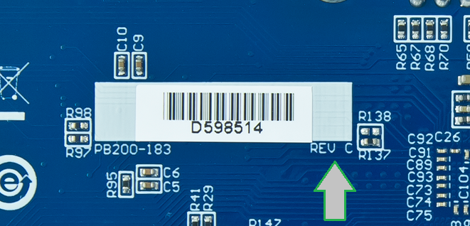
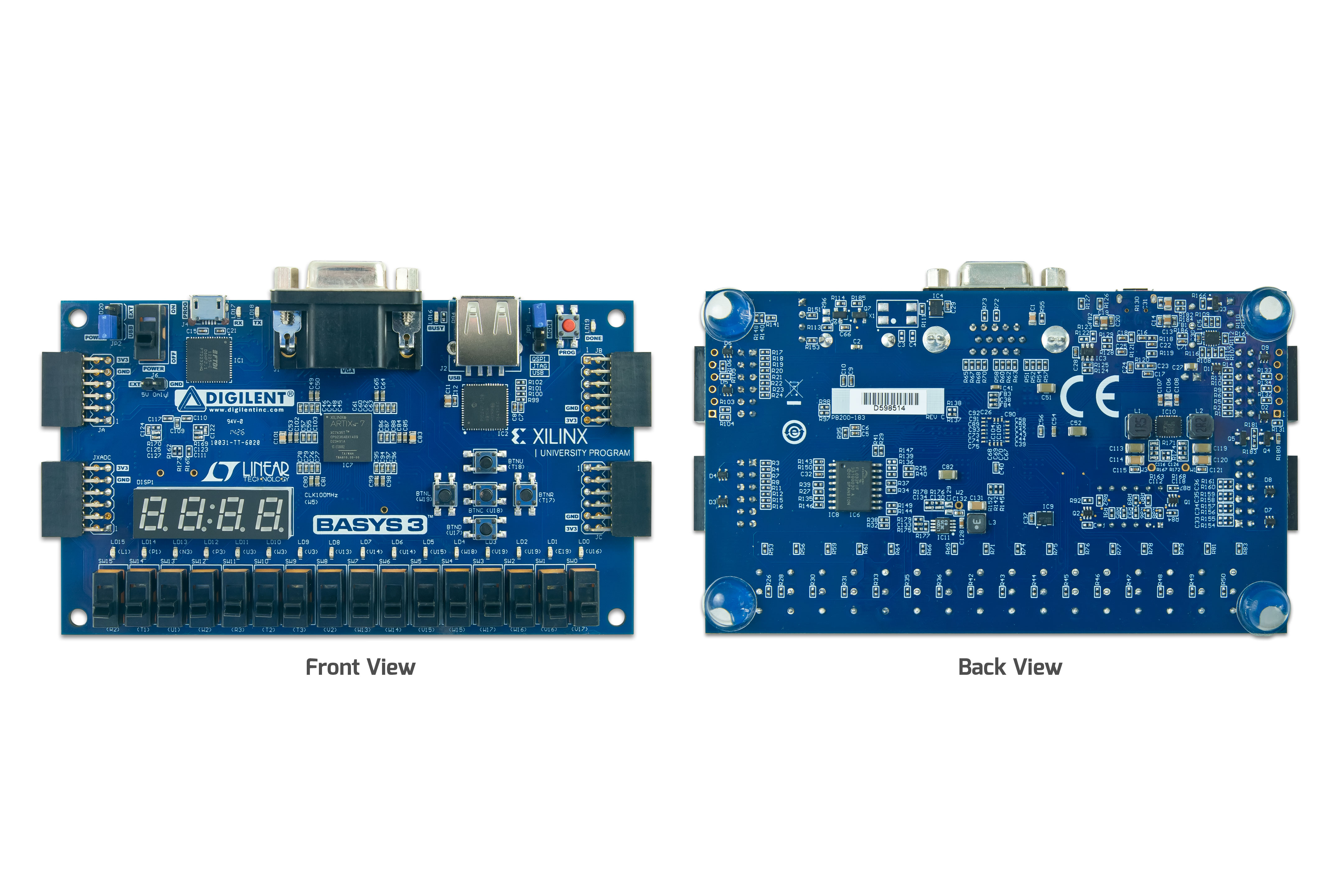
We are on Revision C of the Basys3, no other released versions are currently out. You can find the revision of your board by looking on the underside, near the white bar-coded box.
Overview
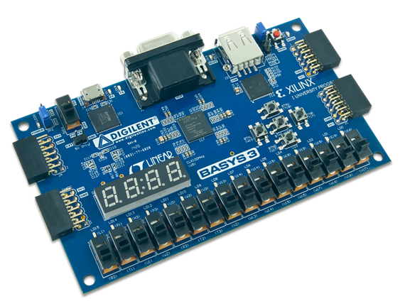
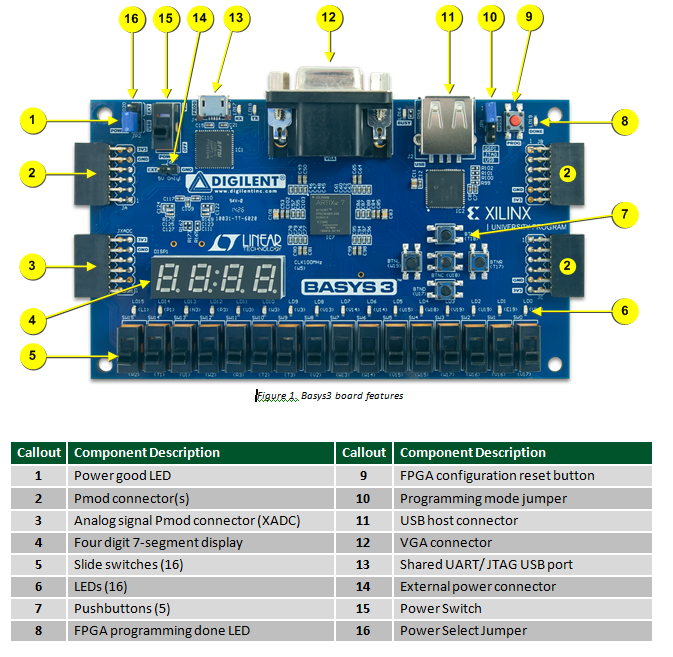
The Basys3 board is a complete, ready-to-use digital circuit development platform based on the latest Artix-7™ Field Programmable Gate Array (FPGA) from Xilinx. With its high-capacity FPGA (Xilinx part number XC7A35T-1CPG236C https://docs.xilinx.com/v/u/en-US/ds181_Artix_7_Data_Sheet), low overall cost, and collection of USB, VGA, and other ports, the Basys3 can host designs ranging from introductory combinational circuits to complex sequential circuits like embedded processors and controllers. It includes enough switches, LEDs and other I/O devices to allow a large number designs to be completed without the need for any additional hardware, and enough uncommitted FPGA I/O pins to allow designs to be expanded using Digilent Pmods or other custom boards and circuits.
The Artix-7 FPGA is optimized for high performance logic, and offers more capacity, higher performance, and more resources than earlier designs. Artix-7 35T features include:
- 33,280 logic cells in 5200 slices (each slice contains four 6-input LUTs and 8 flip-flops);
- 1,800 Kbits of fast block RAM;
- Five clock management tiles, each with a phase-locked loop (PLL);
- 90 DSP slices;
- Internal clock speeds exceeding 450MHz;
- On-chip analog-to-digital converter (XADC).
The Basys3 also offers an improved collection of ports and peripherals, including:
- 16 user switches
- 16 user LEDs
- 5 user pushbuttons
- 4-digit 7-segment display
- Three Pmod ports
- Pmod for XADC signals
- 12-bit VGA output
- USB-UART Bridge
- Serial Flash
- Digilent USB-JTAG port for FPGA programming and communication
- USB HID Host for mice, keyboards and memory sticks
Software--The first Vivado Design Suite Exclusive:
The Basys3 works with Xilinx’s new high-performance Vivado ® Design Suite. Vivado includes many new tools and design flows that facilitate and enhance the latest design methods. It runs faster, allows better use of FPGA resources, and allows designers to focus their time evaluating design alternatives. The System Edition includes an on-chip logic analyzer, high-level synthesis tool, and other cutting-edge tools, and the free “Webpack” version allows Basys3 designs to be created at no additional cost.
Walk Around the Board
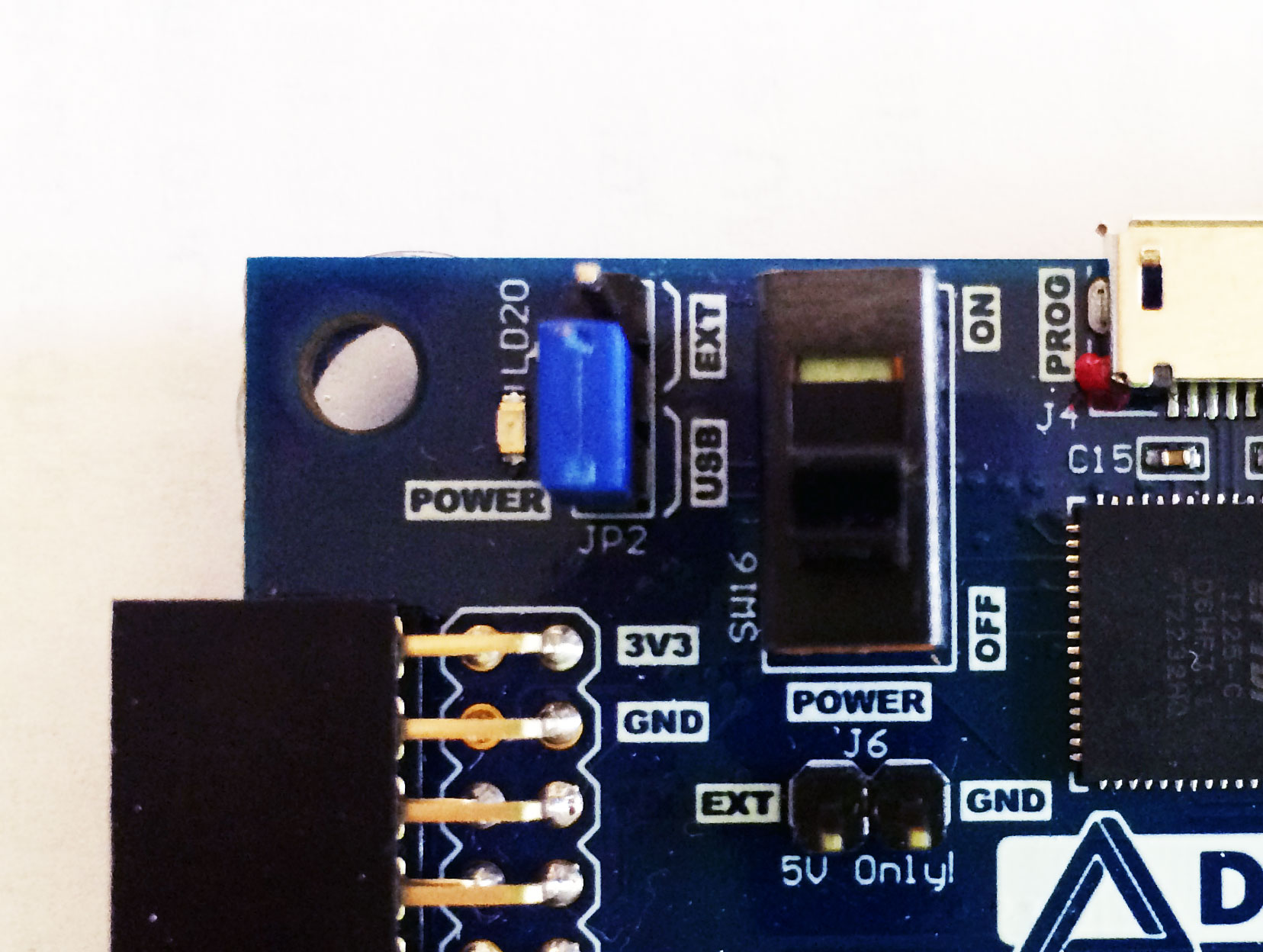
Power
All Basys3 power supplies can be turned on and off by a single logic-level power switch (SW16). A power-good LED (LD20), driven by the “power good” output of the Linear Technologies LTC3633 http://www.linear.com/product/LTC3633 supply, indicates that the supplies are turned on and operating normally. An overview of the Basys3 power circuit is shown below.
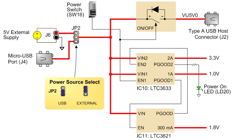
The Basys3 board can receive power from the Digilent USB-JTAG port (J4) or from a 5 volt external power supply (not included). Jumper JP2 (near the power switch) determines which source is used.
USB Power is selected
 The USB port can deliver enough power for the vast majority of designs. A few demanding applications, including any that drive multiple peripheral boards, might require more power than the USB port can provide. Also, some applications may need to run without being connected to a PC’s USB port. In these instances an external power supply or battery pack can be used.
External Power is selected
An external power supply can be used by plugging into the external power header (J6) and setting jumper JP2 to “EXT”. The supply must deliver 4.5VDC to 5.5VDC and at least 1A of current (i.e., at least 5W of power). Many suitable supplies can be purchased through Digikey or other catalog vendors. An external battery pack can be used by connecting the battery’s positive terminal to the “EXT” pin of J6 and the negative terminal to the “GND” pin of J6.
 The power provided to USB devices that are connected to Host connector J2 is not regulated. Therefore it is necessary to limit the maximum voltage of an external battery pack to 5.5V DC. The minimum voltage of the battery pack depends on the application -if the USB Host function (J2) is used, at least 4.6V needs to be provided. In other cases the minimum voltage is 3.6V.
Linear Technology LTC3663
The voltage regulator chosen for the power supply on the Basys 3 is the LTC3663 for the main board power and was chosen to create the required 3.3, 1.8V and 1.0V supplies from the main 5V power input). The auxiliary and RAM functions of the FPGA use the LTC3621 chip. Referring to the below table provides additional information as to the typical currents and values that are needed. However, keep in mind that this has largely to do with FPGA configuration and the values that are provided are given with parameters of a medium sized or speed design.
| Supply | Circuits | Device | Current (max/typical) |
|---|---|---|---|
| 3.3V | FPGA I/O, USB ports, Clocks, Flash, PMODs | IC10: LTC3633 | 2A/0.1 to 1.5A |
| 1.0V | FPGA Core | IC10: LTC3633 | 2A/ 0.2 to 1.3A |
| 1.8V | FPGA Auxiliary and Ram | IC11: LTC3621 | 300mA/ 0.05 to 0.15A |
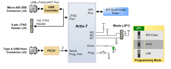
FPGA Configurations
After power-on, the Artix-7 FPGA must be configured (or programmed) before it can perform any functions. To configure the FPGA, you have the option of one of three ways.
- 1. A PC can use the Digilent USB-JTAG circuitry (portJ4, labeled “PROG”) to program the FPGA any time the power is on.
- 2. A file stored in the nonvolatile serial (SPI) flash device can be transferred to the FPGA using the SPI port.
- 3. A programming file can be transferred from a USB memory stick attached to the USB HID port.
The FPGA configuration data is stored in files called bitstreams that have the .bit file extension. The Vivado software from Xilinx can create bitstreams from VHDL, Verilog, or schematic-based source files. Bitstreams are stored in SRAM-based memory cells within the FPGA. This data defines the FPGA’s logic functions and circuit connections, and it remains valid until it is erased by removing board power, by pressing the reset button attached to the PROG input, or by writing a new configuration file using the JTAG port.
An Artix-7 35T bitstream is typically 17,536,096 bits and can take a long time to transfer. The time it takes to program the Basys3 can be decreased by compressing the bitstream before programming, and then allowing the FPGA to decompress the bitsream itself during configuration. Depending on design complexity, compression ratios of 10x can be achieved. Bitstream compression can be enabled within the Xilinx tools (Vivado) to occur during generation. For instructions on how to do this, consult the Xilinx documentation for the toolset being used. After being successfully programmed, the FPGA will cause the “DONE” LED to illuminate. Pressing the “PROG” button at any time will reset the configuration memory in the FPGA.
After being reset, the FPGA will immediately attempt to reprogram itself from whatever method has been selected by the programming mode jumper. The following sections provide greater detail about programming the Basys3 using the different methods available.
JTAG Programming
 The Xilinx tools typically communicate with FPGAs using the Test Access Port and Boundary-Scan Architecture, commonly referred to as JTAG. During JTAG programming, a .bit file is transferred from the PC to the FPGA using the onboard Digilent USB-JTAG circuitry (port J4) or an external JTAG programmer, such as the Digilent JTAG-HS2, attached to port J5 (located below port JA). You can perform JTAG programming any time after the Basys3 has been powered on, regardless of what the mode jumper (JP1) is set to. If the FPGA is already configured, then the existing configuration is overwritten with the bitstream being transmitted over JTAG. Setting the mode jumper to the JTAG setting (seen in Fig 3) is useful to prevent the FPGA from being configured from any other bitstream source until a JTAG programming occurs.
Programming the Basys3 with an uncompressed bitstream using the on-board USB_JTAG circuitry usually takes around five seconds. JTAG programming can be done using the hardware server in Vivado. The demonstration project available at digilentinc.com provides an in-depth tutorial on how to program your board.
The Xilinx tools typically communicate with FPGAs using the Test Access Port and Boundary-Scan Architecture, commonly referred to as JTAG. During JTAG programming, a .bit file is transferred from the PC to the FPGA using the onboard Digilent USB-JTAG circuitry (port J4) or an external JTAG programmer, such as the Digilent JTAG-HS2, attached to port J5 (located below port JA). You can perform JTAG programming any time after the Basys3 has been powered on, regardless of what the mode jumper (JP1) is set to. If the FPGA is already configured, then the existing configuration is overwritten with the bitstream being transmitted over JTAG. Setting the mode jumper to the JTAG setting (seen in Fig 3) is useful to prevent the FPGA from being configured from any other bitstream source until a JTAG programming occurs.
Programming the Basys3 with an uncompressed bitstream using the on-board USB_JTAG circuitry usually takes around five seconds. JTAG programming can be done using the hardware server in Vivado. The demonstration project available at digilentinc.com provides an in-depth tutorial on how to program your board.
Quad SPI Programming
 When programming a nonvolatile flash device, a bitstream file is transferred to the flash in a two-step process. First, the FPGA is programmed with a circuit that can program flash devices, and then data is transferred to the flash device via the FPGA circuit (this complexity is hidden from the user by the Xilinx tools). After the flash device has been programmed, it can automatically configure the FPGA at a subsequent power-on or reset event as determined by the mode jumper setting (see Fig 3). Programming files stored in the flash device will remain until they are overwritten, regardless of power-cycle events.
Programming the flash can take as long as one or two minutes, which is mostly due to the lengthy erase process inherent to the memory technology. Once written however, FPGA configuration can be very fast– less than a second. Bitstream compression, SPI bus width, and configuration rate are factors controlled by the Xilinx tools that can affect configuration speed.
Quad-SPI programming can be performed using Vivado.
When programming a nonvolatile flash device, a bitstream file is transferred to the flash in a two-step process. First, the FPGA is programmed with a circuit that can program flash devices, and then data is transferred to the flash device via the FPGA circuit (this complexity is hidden from the user by the Xilinx tools). After the flash device has been programmed, it can automatically configure the FPGA at a subsequent power-on or reset event as determined by the mode jumper setting (see Fig 3). Programming files stored in the flash device will remain until they are overwritten, regardless of power-cycle events.
Programming the flash can take as long as one or two minutes, which is mostly due to the lengthy erase process inherent to the memory technology. Once written however, FPGA configuration can be very fast– less than a second. Bitstream compression, SPI bus width, and configuration rate are factors controlled by the Xilinx tools that can affect configuration speed.
Quad-SPI programming can be performed using Vivado.
USB Host Programming
You can program the FPGA from a pen drive attached to the USB-HID port (J2) by doing the following:
- 1. Format the storage device (Pen drive) with a FAT32 file system.
- 2. Place a single .bit configuration file in the root directory of the storage device.
- 3. Attach the storage device to the Basys3.
- 4. Set the JP1 Programming Mode jumper on the Basys3 to “USB”.
- 5. Push the PROG button or power-cycle the Basys3.
The FPGA will automatically be configured with the .bit file on the selected storage device. Any .bit files that are not built for the proper Artix-7 device will be rejected by the FPGA. The Auxiliary Function Status, or “BUSY” LED (LD16), gives visual feedback on the state of the configuration process when the FPGA is not yet programmed:
- When steadily lit the auxiliary microcontroller is either booting up or currently reading the configuration medium (pen drive) and downloading a bitstream to the FPGA.
- A slow pulse means the microcontroller is waiting for a configuration medium to be plugged in.
- In case of an error during configuration the LED will blink rapidly.
When the FPGA has been successfully configured, the behavior of the LED is application-specific. For example, if a USB keyboard is plugged in, a rapid blink will signal the receipt of an HID input report from the keyboard.
Memory
 The Basys3 board contains a 32Mbit non-volatile serial Flash device, which is attached to the Artix 7 FPGA using a dedicated quad-mode (x4) SPI bus. The connections and pin assignments between the FPGA and the serial flash device are shown the below figure.
FPGA configuration files can be written to the Quad SPI Flash (Spansion part number S25FL032), and mode settings are available to cause the FPGA to automatically read a configuration from this device at power on. An Artix-7 35T configuration file requires just over two Mbytes of memory, leaving approximately 48% of the flash device available for user data.
For more information about this particular chip please refer to the Spansion DataSheet: https://www.spansion.com/Support/Datasheets/S25FL032P_00.pdf
Oscillators/ Clocks
The Basys3 board includes a single 100MHz oscillator connected to pin W5 (W5 is a MRCC input on bank 34). The input clock can drive MMCMs or PLLs to generate clocks of various frequencies and with known phase relationships that may be needed throughout a design. Some rules restrict which MMCMs and PLLs may be driven by the 100MHz input clock. For a full description of these rules and of the capabilities of the Artix-7 clocking resources, refer to the “7 Series FPGAs Clocking Resources User Guide” available from Xilinx https://docs.xilinx.com/v/u/en-US/ug472_7Series_Clocking.
Xilinx offers the Clocking Wizard IP core to help users generate the different clocks required for a specific design. This wizard properly instantiates the needed MMCMs and PLLs based on the desired frequencies and phase relationships specified by the user. The wizard will then output an easy to use wrapper component around these clocking resources that can be inserted into the user’s design. The Clocking Wizard can be accessed from within IP Catalog, which can be found under the Project Manager section of the Flow Navigator in Vivado.
USB-UART Bridge (Serial Port)
The Basys3 includes an FTDI FT2232HQ http://www.ftdichip.com/Support/Documents/DataSheets/ICs/DS_FT2232H.pdf USB-UART bridge (attached to connector J4) that allows you to use PC applications to communicate with the board using standard Windows COM port commands. Free USB-COM port drivers, available from www.ftdichip.com under the “Virtual Com Port” or VCP heading, convert USB packets to UART/serial port data. Serial port data is exchanged with the FPGA using a two-wire serial port (TXD/RXD). After the drivers are installed, I/O commands can be used from the PC directed to the COM port to produce serial data traffic on the B18 and A18 FPGA pins.
Two on-board status LEDs provide visual feedback on traffic flowing through the port: the transmit LED (LD18) and the receive LED (LD17). Signal names that imply direction are from the point-of-view of the DTE (Data Terminal Equipment), in this case the PC.
The FT2232HQ is also used as the controller for the Digilent USB-JTAG circuitry, but the USB-UART and USB-JTAG functions behave entirely independent of one another. Programmers interested in using the UART functionality of the FT2232 within their design do not need to worry about the JTAG circuitry interfering with the UART data transfers, and vice-versa. The combination of these two features into a single device allows the Basys3 to be programmed, communicated with via UART, and powered from a computer attached with a single Micro USB cable. The connections between the FT2232HQ and the Artix-7 are shown in the below figure.
USB HID Host
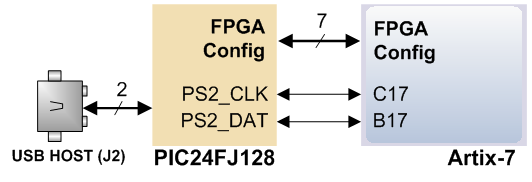
The Auxiliary Function microcontroller (Microchip PIC24FJ128 http://ww1.microchip.com/downloads/en/DeviceDoc/39747C.pdf) provides the Basys3 with USB HID host capability.
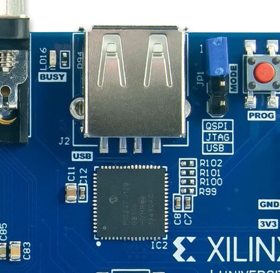
After power-up, the microcontroller is in configuration mode, either downloading a bitstream to the FPGA, or waiting for it to be programmed from other sources. Once the FPGA is programmed, the microcontroller switches to application mode, which, in this case, is USB HID Host mode. Firmware in the microcontroller can drive a mouse or a keyboard attached to the type A USB connector at J2 labeled “USB.” Hub support is not currently available, so only a single mouse or a single keyboard can be used. The PIC24 drives several signals into the FPGA – two are used to implement a standard PS/2 interface for communication with a mouse or keyboard, and the others are connected to the FPGA’s two-wire serial programming port, so the FPGA can be programmed from a file stored on a USB pen drive.
HID Controller
The Auxiliary Function microcontroller hides the USB HID protocol from the FPGA and emulates an old-style PS/2 bus. The microcontroller behaves just like a PS/2 keyboard or mouse would. This means new designs can re-use existing PS/2 IP cores. Mice and keyboards that use the PS/2 protocol use a two-wire serial bus (clock and data) to communicate with a host. On the Basys3, the microcontroller emulates a PS/2 device while the FPGA plays the role of the host. Both the mouse and the keyboard use 11-bit words that include a start bit, data byte (LSB first), odd parity, and stop bit, but the data packets are organized differently, and the keyboard interface allows bi-directional data transfers (so the host device can illuminate state LEDs on the keyboard). Bus timings are shown in the below figure.
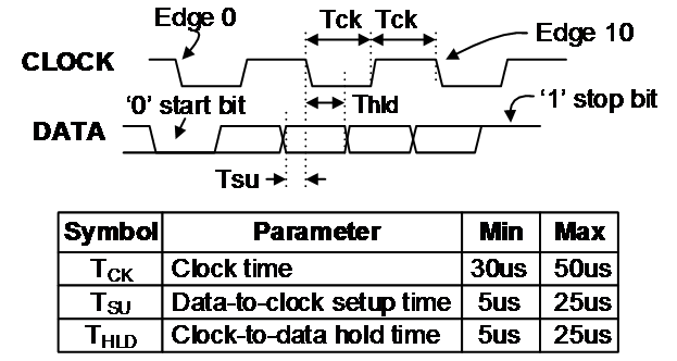
The clock and data signals are only driven when data transfers occur; otherwise they are held in the idle state at logic ‘1.’ This requires that when the PS/2 signals are used in a design, internal pull-ups must be enabled in the FPGA on the data and clock pins. The clock signal is normally driven by the device, but may be held low by the host in special cases. The timings define signal requirements for mouse-to-host communications and bi-directional keyboard communications. A PS/2 interface circuit can be implemented in the FPGA to create a keyboard or mouse interface.
When a keyboard or mouse is connected to the Basys3, a “self-test passed” command (0xAA) is sent to the host. After this, commands may be issued to the device. Since both the keyboard and the mouse use the same PS/2 port, one can tell the type of device connected using the device ID. This ID can be read by issuing a Read ID command (0xF2). Also, a mouse sends its ID (0x00) right after the “self-test passed” command, which distinguishes it from a keyboard.
Keyboard
The keyboard uses open-collector drivers so the keyboard, or an attached host device, can drive the two-wire bus (if the host device will not send data to the keyboard, then the host can use input-only ports).
PS/2-style keyboards use scan codes to communicate key press data. Each key is assigned a code that is sent whenever the key is pressed. If the key is held down, the scan code will be sent repeatedly about once every 100ms. When a key is released, an F0 key-up code is sent, followed by the scan code of the released key. If a key can be shifted to produce a new character (like a capital letter), then a shift character is sent in addition to the scan code, and the host must determine which ASCII character to use. Some keys, called extended keys, send an E0 ahead of the scan code (and they may send more than one scan code). When an extended key is released, an E0 F0 key-up code is sent, followed by the scan code. Scan codes for most keys are shown in the below figure.

A host device can also send data to the keyboard. The keyboard can send data to the host only when both the data and clock lines are high (or idle). Because the host is the bus master, the keyboard must check to see whether the host is sending data before driving the bus. To facilitate this, the clock line is used as a “clear to send” signal. If the host drives the clock line low, the keyboard must not send any data until the clock is released. The keyboard sends data to the host in 11-bit words that contain a ‘0’ start bit, followed by 8-bits of scan code (LSB first), followed by an odd parity bit and terminated with a ‘1’ stop bit. The keyboard generates 11 clock transitions (at 20 to 30KHz) when the data is sent, and data is valid on the falling edge of the clock.
| Command | Action |
|---|---|
| ED | Set Num Lock, Caps Lock, and Scroll Lock LEDs. Keyboard returns FA after receiving ED, then host sends a byte to set LED status: bit 0 sets Scroll Lock, bit 1 sets Num Lock, and bit 2 sets Caps lock. Bits 3 to 7 are ignored. |
| EE | Echo (test). Keyboard returns EE after receiving EE |
| F3 | Set scan code repeat rate. Keyboard returns F3 on receiving FA, then host sends second byte to set the repeat rate. |
| FE | Resend. FE directs keyboard to re-send most recent scan code. |
| FF | Reset. Resets the keyboard. |
Mouse
Once entered in stream mode and data reporting has been enabled, the mouse outputs a clock and data signal when it is moved: otherwise, these signals remain at logic ‘1.’ Each time the mouse is moved, three 11-bit words are sent from the mouse to the host device, as shown in Fig 10. Each of the 11-bit words contains a ‘0’ start bit, followed by 8 bits of data (LSB first), followed by an odd parity bit, and terminated with a ‘1’ stop bit. Thus, each data transmission contains 33 bits, where bits 0, 11, and 22 are ‘0’ start bits, and bits 11, 21, and 33 are ‘1’ stop bits. The three 8-bit data fields contain movement data as shown in the below figure. Data is valid at the falling edge of the clock, and the clock period is 20 to 30KHz.
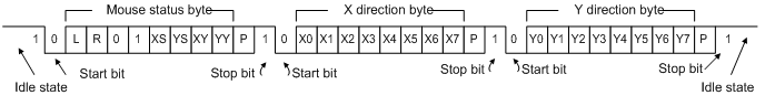
The mouse assumes a relative coordinate system wherein moving the mouse to the right generates a positive number in the X field, and moving to the left generates a negative number. Likewise, moving the mouse up generates a positive number in the Y field, and moving down represents a negative number (the XS and YS bits in the status byte are the sign bits – a ‘1’ indicates a negative number). The magnitude of the X and Y numbers represent the rate of mouse movement – the larger the number, the faster the mouse is moving (the XV and YV bits in the status byte are movement overflow indicators – a ‘1’ means overflow has occurred). If the mouse moves continuously, the 33-bit transmissions are repeated every 50ms or so. The L and R fields in the status byte indicate Left and Right button presses (a ‘1’ indicates the button is being pressed).
The microcontroller also supports Microsoft Intellimouse-type extensions for reporting back a third axis representing the mouse wheel, as shown in the below table.
| Command | Action |
|---|---|
| EA | Set stream mode. The mouse responds with “acknowledge” (0xFA) then resets its movement counters and enters stream mode. |
| F4 | Enable data reporting. The mouse responds with “acknowledge” (0xFA) then enables data reporting and resets its movement counters. This command only affects behavior in stream mode. Once issued, mouse movement will automatically generate a data packet. |
| F5 | Disable data reporting. The mouse responds with “acknowledge” (0xFA) then disables data reporting and resets its movement counters. |
| F3 | Set mouse sample rate. The mouse responds with “acknowledge” (0xFA) then reads one more byte from the host. This byte is then saved as the new sample rate, and a new “acknowledge” packet is issued. |
| FE | Resend. FE directs mouse to re-send last packet. |
| FF | Reset. The mouse responds with “acknowledge” (0xFA) then enters reset mode. |
VGA Port
The Basys3 board uses 14 FPGA signals to create a VGA port with 4 bits-per-color and the two standard sync signals (HS – Horizontal Sync, and VS – Vertical Sync). The color signals use resistor-divider circuits that work in conjunction with the 75-ohm termination resistance of the VGA display to create 16 signal levels each on the red, green, and blue VGA signals.
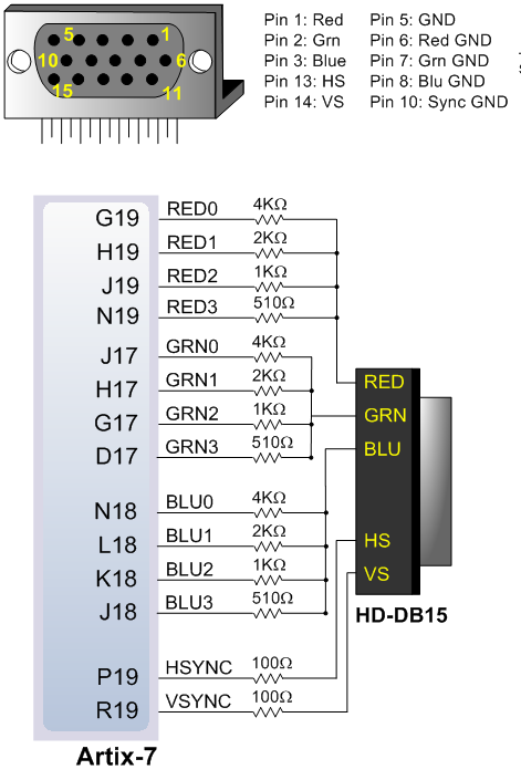
This circuit, shown in the above diagram, , produces video color signals that proceed in equal increments between 0V (fully off) and 0.7V (fully on). Using this circuit, 4096 different colors can be displayed, one for each unique 12-bit pattern. A video controller circuit must be created in the FPGA to drive the sync and color signals with the correct timing in order to produce a working display system.
 A helpful way to understand the way that VGA signals are transmitted is to understand the method of which CRT (Cathode Ray Tubes) function for displaying images. Although the technology may seem outdated, it is from this legacy that many of the signal names and timings have arisen.
The below section can also be found in the Nexys4 reference manual.
VGA System Timing (taken from the Nexys4 reference manual)
VGA signal timings are specified, published, copyrighted, and sold by the VESA organization (www.vesa.org). The following VGA system timing information is provided as an example of how a VGA monitor might be driven in 640 by 480 mode. NOTE: For more precise information, or for information on other VGA frequencies, refer to documentation available at the VESA website.
How CRT Displays Work- Theory
CRT-based VGA displays use amplitude-modulated moving electron beams (or cathode rays) to display information on a phosphor-coated screen. LCD displays use an array of switches that can impose a voltage across a small amount of liquid crystal, thereby changing light permittivity through the crystal on a pixel-by-pixel basis. Although the following description is limited to CRT displays, LCD displays have evolved to use the same signal timings as CRT displays (so the “signals” discussion below pertains to both CRTs and LCDs). Color CRT displays use three electron beams (one for red, one for blue, and one for green) to energize the phosphor that coats the inner side of the display end of a cathode ray tube.
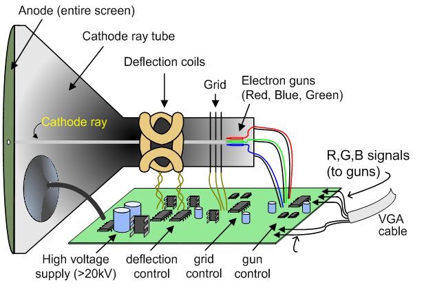
Electron beams emanate from “electron guns” which are finely-pointed heated cathodes placed in close proximity to a positively charged annular plate called a “grid.” The electrostatic force imposed by the grid pulls rays of energized electrons from the cathodes, and those rays are fed by the current that flows into the cathodes. These particle rays are initially accelerated towards the grid, but they soon fall under the influence of the much larger electrostatic force that results from the entire phosphor-coated display surface of the CRT being charged to 20kV (or more). The rays are focused to a fine beam as they pass through the center of the grids, and then they accelerate to impact on the phosphor-coated display surface. The phosphor surface glows brightly at the impact point, and it continues to glow for several hundred microseconds after the beam is removed. The larger the current fed into the cathode, the brighter the phosphor will glow.
Between the grid and the display surface, the beam passes through the neck of the CRT where two coils of wire produce orthogonal electromagnetic fields. Because cathode rays are composed of charged particles (electrons), they can be deflected by these magnetic fields. Current waveforms are passed through the coils to produce magnetic fields that interact with the cathode rays and cause them to transverse the display surface in a “raster” pattern, horizontally from left to right and vertically from top to bottom, as shown in the below figure. As the cathode ray moves over the surface of the display, the current sent to the electron guns can be increased or decreased to change the brightness of the display at the cathode ray impact point.
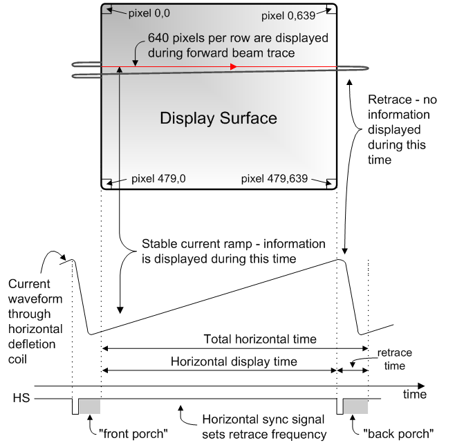
Video data typically comes from a video refresh memory, with one or more bytes assigned to each pixel location (the Basys3 uses 12 bits per pixel). The controller must index into video memory as the beams move across the display, and retrieve and apply video data to the display at precisely the time the electron beam is moving across a given pixel.
A VGA controller circuit must generate the HS and VS timings signals and coordinate the delivery of video data based on the pixel clock. The pixel clock defines the time available to display one pixel of information. The VS signal defines the “refresh” frequency of the display, or the frequency at which all information on the display is redrawn. The minimum refresh frequency is a function of the display’s phosphor and electron beam intensity, with practical refresh frequencies falling in the 50Hz to 120Hz range. The number of lines to be displayed at a given refresh frequency defines the horizontal “retrace” frequency. For a 640-pixel by 480-row display using a 25MHz pixel clock and 60 +/-1Hz refresh, the signal timings shown in below figure can be derived. Timings for sync pulse width and front and back porch intervals (porch intervals are the pre- and post-sync pulse times during which information cannot be displayed) are based on observations taken from actual VGA displays.

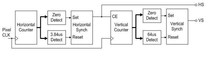
A VGA controller circuit, such as the one diagramed in the below, decodes the output of a horizontal-sync counter driven by the pixel clock to generate HS signal timings. You can use this counter to locate any pixel location on a given row. Likewise, the output of a vertical-sync counter that increments with each HS pulse can be used to generate VS signal timings, and you can use this counter to locate any given row. These two continually running counters can be used to form an address into video RAM. No time relationship between the onset of the HS pulse and the onset of the VS pulse is specified, so you can arrange the counters to easily form video RAM addresses, or to minimize decoding logic for sync pulse generation.
Basic I/O
The Basys3 board includes sixteen slide switches, five push buttons, sixteen individual LEDs, and a four-digit seven-segment display, as shown in the below diagram. The pushbuttons and slide switches are connected to the FPGA via series resistors to prevent damage from inadvertent short circuits (a short circuit could occur if an FPGA pin assigned to a pushbutton or slide switch was inadvertently defined as an output). The five pushbuttons, arranged in a plus-sign configuration, are “momentary” switches that normally generate a low output when they are at rest, and a high output only when they are pressed. Slide switches generate constant high or low inputs depending on their position.

The sixteen individual high-efficiency LEDs are anode-connected to the FPGA via 330-ohm resistors, so they will turn on when a logic high voltage is applied to their respective I/O pin. Additional LEDs, which are not user-accessible, indicate power-on, FPGA programming status, and USB port status.
Seven Segment Display
The Basys3 board contains one four-digit common anode seven-segment LED display. Each of the four digits is composed of seven segments arranged in a “figure 8” pattern, with an LED embedded in each segment. Segment LEDs can be individually illuminated, so any one of 128 patterns can be displayed on a digit by illuminating certain LED segments and leaving the others dark, as shown in the below. Of these 128 possible patterns, the ten corresponding to the decimal digits are the most useful.

The anodes of the seven LEDs forming each digit are tied together into one “common anode” circuit node, but the LED cathodes remain separate, as shown in Fig 18. The common anode signals are available as four “digit enable” input signals to the 4-digit display. The cathodes of similar segments on all four displays are connected into seven circuit nodes labeled CA through CG (so, for example, the four “D” cathodes from the four digits are grouped together into a single circuit node called “CD”). These seven cathode signals are available as inputs to the 4-digit display. This signal connection scheme creates a multiplexed display, where the cathode signals are common to all digits but they can only illuminate the segments of the digit whose corresponding anode signal is asserted.

To illuminate a segment, the anode should be driven high while the cathode is driven low. However, since the Basys3 uses transistors to drive enough current into the common anode point, the anode enables are inverted. Therefore, both the AN0..3 and the CA..G/DP signals are driven low when active.
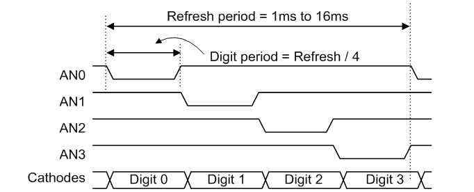
A scanning display controller circuit can be used to show a four-digit number on this display. This circuit drives the anode signals and corresponding cathode patterns of each digit in a repeating, continuous succession at an update rate that is faster than the human eye can detect. Each digit is illuminated just one-fourth of the time, but because the eye cannot perceive the darkening of a digit before it is illuminated again, the digit appears continuously illuminated. If the update, or “refresh”, rate is slowed to around 45 hertz, a flicker can be noticed in the display.
For each of the four digits to appear bright and continuously illuminated, all four digits should be driven once every 1 to 16ms, for a refresh frequency of about 1KHz to 60Hz. For example, in a 62.5Hz refresh scheme, the entire display would be refreshed once every 16ms, and each digit would be illuminated for 1/4 of the refresh cycle, or 4ms. The controller must drive low the cathodes with the correct pattern when the corresponding anode signal is driven high. To illustrate the process, if AN0 is asserted while CB and CC are asserted, then a “1” will be displayed in digit position 1. Then, if AN1 is asserted while CA, CB, and CC are asserted, a “7” will be displayed in digit position 2. If AN0, CB, and CC are driven for 4ms, and then AN1, CA, CB, and CC are driven for 4ms in an endless succession, the display will show “71” in the first two digits. An example timing diagram for a four-digit controller is shown below.
Pmod Ports

A major change from the Basys2 to the Basys3 is the addition of double row Pmod ports. Digilent produces a large collection of Pmod (Peripheral Module) accessory boards that can attach to the expansion ports to add ready-made functions such as A/D's, D/A's, motor drivers, sensors, displays, and many other functions. These ports can be used as simple expansion ports, since all of the pin-outs correspond to pins on the FPGA.
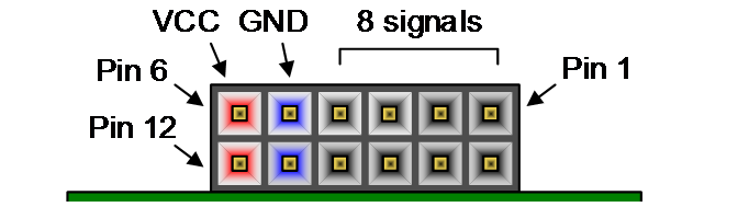
The Pmod ports are arranged in a 2×6 right-angle, and are 100-mil female connectors that mate with standard 2×6 pin headers. Each 12-pin Pmod ports provides two 3.3V VCC signals (pins 6 and 12), two Ground signals (pins 5 and 11), and eight logic signals, as shown in Fig 20. The VCC and Ground pins can deliver up to 1A of current. Pmod data signals are not matched pairs, and they are routed using best-available tracks without impedance control or delay matching. Pin assignments for the Pmod I/O connected to the FPGA are shown in the below table.
| Pmod JA | Pmod JB | Pmod JC | Pmod JXADC |
|---|---|---|---|
| JA1: J1 | JB1: A14 | JC1: K17 | JXADC1: J3 |
| JA2: L2 | JB2: A16 | JC2: M18 | JXADC2: L3 |
| JA3: J2 | JB3: B15 | JC3: N17 | JXADC3: M2 |
| JA4: G2 | JB4: B16 | JC4: P18 | JXADC4: N2 |
| JA7: H1 | JB7: A15 | JC7: L17 | JXADC7: K3 |
| JA8: K2 | JB8: A17 | JC8: M19 | JXADC8: M3 |
| JA9: H2 | JB9: C15 | JC9: P17 | JXADC9: M1 |
| JA10: G3 | JB10: C16 | JC10: R18 | JXADC10: N1 |
The signals in the table correspond to physical pins on the FPGA. These are used to create the net names for the FPGA. These should be available in the XDC file in Vivado.

Dual Analog/Digital Pmod (JXADC)
 The on-board Pmod expansion port labeled “JXADC” is wired to the auxiliary analog input pins of the FPGA. Depending on the configuration, this port can be used to input differential analog signals to the analog-to-digital converter inside the Artix-7 (XADC). Any or all pairs in the port can be configured either as analog input or digital input-output.
The Dual Analog/Digital Pmod on the Basys3 differs from the rest in the routing of its traces. The eight data signals are grouped into four pairs, with the pairs routed closely coupled for better analog noise immunity. Furthermore, each pair has a partially loaded anti-alias filter laid out on the PCB. The filter does not have capacitors C33-C36. In designs where such filters are desired, the capacitors can be manually loaded by the user.
The on-board Pmod expansion port labeled “JXADC” is wired to the auxiliary analog input pins of the FPGA. Depending on the configuration, this port can be used to input differential analog signals to the analog-to-digital converter inside the Artix-7 (XADC). Any or all pairs in the port can be configured either as analog input or digital input-output.
The Dual Analog/Digital Pmod on the Basys3 differs from the rest in the routing of its traces. The eight data signals are grouped into four pairs, with the pairs routed closely coupled for better analog noise immunity. Furthermore, each pair has a partially loaded anti-alias filter laid out on the PCB. The filter does not have capacitors C33-C36. In designs where such filters are desired, the capacitors can be manually loaded by the user.
:!:NOTE: The coupled routing and the anti-alias filters might limit the data speeds when used for digital signals. The XADC core within the Artix-7 is a dual channel 12-bit analog-to-digital converter capable of operating at 1 MSPS.
Either channel can be driven by any of the auxiliary analog input pairs connected to the JXADC header. The XADC core is controlled and accessed from a user design via the Dynamic Reconfiguration Port (DRP). The DRP also provides access to voltage monitors that are present on each of the FPGA’s power rails, and a temperature sensor that is internal to the FPGA. For more information on using the XADC core, refer to the Xilinx document titled “7 Series FPGAs and Zynq-7000 All Programmable SoC XADC Dual 12-Bit 1 MSPS Analog-to-Digital Converter.”: https://docs.xilinx.com/v/u/en-US/ug480_7Series_XADC
Built in Self Test
A demonstration configuration is loaded into the SPI Flash device on the Basys3 board during manufacturing. The source code and prebuilt bitstream for this design are available for download from the Digilent website. If the demo configuration is present in the SPI Flash device and the Basys3 board is powered on in SPI mode, the demo project will allow basic hardware verification. Here is an overview of how this demo drives the different onboard components:
- The user LEDs are illuminated when the corresponding user switch is placed in the on position.
- The VGA port displays feedback from a USB Mouse.
- Connecting a mouse to the USB-HID Mouse port will allow the pointer on the VGA display to be controlled.
- On power-up, each digit of the seven-segment display will display a counter output from 0-9 that increments once a second.
- Pressing BTNU, BTNL, BTNR, or BTND will cause a digit of the seven-segment display to go blank.
- Pressing BTNC will reset the design.
- On power-up, a welcome message is sent over the UART. Also, every time a button is pressed a message is sent. The UART can be connected to using a terminal program with 9600 Baud, 8 data bits, 1 stop bit, and no parity.
All Basys3 boards are 100% tested during the manufacturing process. If any device on the Basys3 board fails test or is not responding properly, it is likely that damage occurred during transport or during use. Typical damage includes stressed solder joints and contaminants in switches and buttons resulting in intermittent failures. Stressed solder joints can be repaired by reheating and reflowing solder and contaminants can be cleaned with off-the-shelf electronics cleaning products. If a board fails test within the warranty period, it will be replaced at no cost.
FAQ for Basys3
 the following section is for the collection of FAQ that is not answered in the reference manual.
What is the difference between the Basys 2 and the Basys 3?
| Basys2 | Basys3 | |
|---|---|---|
| FPGA Family | Spartan (XC3S100E) | Artix (XC7A35T) |
| 2,160 logic cells | 33,280 logic cells | |
| 0 DSP Slices ( 4 Multipliers) | 90 DSP Slices | |
| 72kB BRAM | 1899Kb BRAM | |
| Design Tools | ISE | Vivado |
| On-board USB programming | X | X |
| USB powered | X | X |
| On-board configuration ROM | X | X |
| USB-HID port for mouse and keyboard | X | |
| PS-2 port | X | |
| USB thumb drive for FPGA config and user data | X | |
| USB COM port with Windows and Linux drivers | X | |
| 7-segment display | X | X |
| VGA port | 8- bit, med res | 12 bit, hi res |
| Slide switches | 8 | 16 |
| LEDs | 8 | 16 |
| Push buttons | 4 | 6 |
| Pmods ports | Four Single rows | Four Double rows |
| Analog inputs | 0 | 4 |
| Power switch and power good LED | X | |
| FPGA reset button and DONE LED | X |